

Executive Overview
Artificial intelligence has reached a critical architectural impasse. While generative models, deep neural networks, and autonomous robotics grow exponentially in scale and capability, the hardware infrastructure supporting them is gasping for breath. The core problem is no longer just processing power; it is the physical limitation of moving data. Traditional computing relies on copper wires and electrical buses to shuffle colossal arrays of model parameters between memory banks—such as dynamic RAM (DRAM)—and application processors. As AI models bloat into billions of parameters, these electrical interconnects consume staggering amounts of energy, generate prohibitive heat, and create a severe bandwidth bottleneck.
Enter a radical paradigm shift being forged in a Cornell Tech laboratory in New York City. Researchers Yifan He and Jae-sun Seo have unveiled a groundbreaking optical receiver design that bypasses traditional electrical interconnects entirely. By beaming rapid flashes of light patterned like complex QR codes directly onto modified static RAM (SRAM) cells, the system allows AI processors to update their internal memory parameters "on the fly" using pure photocurrents.
Presented at the IEEE/JSAP Symposium on VLSI Technology & Circuits in Honolulu, this innovation promises to slash the energy footprint of data centers, self-driving cars, and edge-AI applications like warehouse robots. By eliminating the power-hungry analog conversion circuits that have historically plagued optical communications, Cornell Tech’s fully digital, light-based memory-flipping technique could redefine the future of high-performance computing. However, as independent experts point out, scaling this technology from a static lab bench proof-of-concept to a commercially viable silicon chip will require overcoming significant hurdles in manufacturing density and optical transmission speeds.
Detailed Chronology: From Concept to the Honolulu Reveal
The journey toward optically programmable memory began as an attempt to solve a deceptively simple question: Why must light-based data transmission—which moves at blistering speeds with minimal energy loss—be crippled by the electronics required to process it?
The Analog Trap
For years, engineers have understood that optics offer vastly superior bandwidth compared to traditional metal wiring. Fiber-optic cables power global internet backbones because photons do not suffer from the resistance, capacitive drag, and thermal dissipation that hobble electrons in copper wires. Yet, when optical signals reach a computer processor, they hit a brick wall. Traditional optical receivers rely on complex, power-hungry analog-to-digital converters and analog circuits to translate incoming light beams into electrical bits that a processor can understand. The energy saved by transmitting data via light was frequently canceled out by the power required to convert that light at the destination chip.
The Cornell Tech Breakthrough
Recognizing this inefficiency, postdoctoral researcher Yifan He and associate professor Jae-sun Seo conceptualized a wholly different approach: eliminate the analog conversion layer entirely by making the memory cells themselves photosensitive.
Instead of converting light into electronic data via external circuits, the Cornell Tech team modified SRAM cells to integrate microscopic photodiodes. When a directed beam of light strikes these modified cells, the resulting photocurrents directly alter the binary states (the 0s and 1s) within the SRAM memory array.
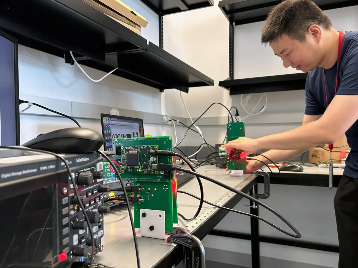
By last year, the team had constructed a working benchtop prototype. Visitors to their laboratory could witness the future of computing in action: a lens positioned nearly a meter away from an LED emitter shining a red light beam toward an optical receiver chip. Attached monitors displayed a shifting matrix of squares resembling an advanced QR code. Unlike a standard smartphone camera reading a QR code merely to open a web browser, the receiver chip in He and Seo’s lab was reading the light matrix to directly overwrite and update its internal memory parameters.
The Honolulu Debut
The culmination of this foundational research was formally presented at the IEEE/JSAP Symposium on VLSI Technology & Circuits in Honolulu. The reception from the international semiconductor community was immediate. By demonstrating that optical communication could be kept entirely digital from transmission to memory storage, the Cornell Tech team offered a tangible blueprint for bypassing the memory wall that currently limits processor scaling.
Supporting Context & Metrics: The Physics of Light-Driven Memory
To understand why this optical breakthrough matters, one must examine the physical realities of modern chip architecture.
SRAM vs. DRAM: The Memory Dilemma
Microprocessors rely on two primary forms of volatile memory:
- Static RAM (SRAM): Blazingly fast and built directly onto the processor die, SRAM houses the active data a chip needs immediately. However, it takes up significant physical space on the silicon, meaning processors can only hold a fraction of a modern AI model’s parameters directly in SRAM.
- Dynamic RAM (DRAM): Located off-chip or on separate stacked dies, DRAM offers vastly higher storage capacities within a smaller footprint, but accessing it introduces latency and consumes substantial electrical power.
When an AI model executes, it constantly pulls weights and parameters from DRAM across electrical interconnects. As models expand to trillions of parameters, these data-shuffling operations choke system throughput.
The Photodiode Advantage
In the Cornell Tech architecture, the division of labor is reimagined. The DRAM storage component remains bundled with the optical transmitter, while the optical receiver is embedded directly into the processor’s SRAM layer.
[ Optical Transmitter + DRAM ]
          │
          │ (Beamed Light Array / QR-like Matrix)
          ▼
[ Optical Receiver + Modified SRAM ]
          │
          ├─► Photodiodes capture light
          ├─► Generated photocurrents "flip" binary bits
          └─► AI Model parameters updated instantly on-chip
When the transmitter beams data down to the SRAM array, photons strike the integrated photodiodes. Each photodiode acts as an optoelectronic switch, generating a precise current that flips the binary values of the underlying memory cells.
Solving the Alignment Challenge
A major engineering hurdle in free-space optical communication is physical alignment. Transmitters and receivers in real-world devices cannot be guaranteed to sit in rigid, perpendicular perfection. To counteract this, the Cornell Tech team engineered a robust calibration framework.
Before streaming live AI model parameters, the chip references an initial data frame containing spatial metadata about the expected position of every pixel in the light matrix. Even if the receiver is tilted or slightly misaligned relative to the LED beam, the onboard calibration circuit dynamically adjusts, ensuring lossless data reception.
Official Statements & Expert Analysis
The implications of this research extend far beyond academic circles, drawing praise—and pragmatic caution—from industry veterans.

"People are designing all sorts of different AI chips. These processors don’t often have room for all the parameters that make up AI models, so the additional data is stored in dynamic RAM. The electrical connections commonly used to move the data between the DRAM and the processor create cost and efficiency concerns when systems scale up. That’s one of the major bottlenecks."
— Jae-sun Seo, Associate Professor of Electrical and Computer Engineering, Cornell Tech
The sentiment is echoed by external observers who recognize the commercial stakes involved in subverting traditional silicon interconnect bottlenecks.
"This is a really important problem. It’s got massive commercial implications. This solution is a clever way of dealing with it."
— Dennis Sylvester, IEEE Fellow and Chair of Electrical and Computer Engineering, University of Michigan
However, Sylvester also injects a necessary dose of engineering realism regarding the path to market. Because the photosensitive bit cells required to capture light are currently larger than traditional, ultra-dense SRAM bit cells, the chip sacrifices some storage capacity.
"The tech in its current form is likely far from commercialization because the individual photosensitive bit cells are larger than SRAM bit cells in conventional chips. Those larger cells mean the chip can fit less memory, a trade-off that could cancel out the added efficiency of the light-based approach."
— Dennis Sylvester
Addressing this critique, Jae-sun Seo notes that his team is actively working to minimize bit-cell dimensions. By optimizing transistor layouts, refining circuit designs, and leveraging advanced complementary metal-oxide-semiconductor (CMOS) scaling, the researchers believe they can shrink the photosensitive elements to competitive commercial sizes.
Future Outlook: Edge AI, Robotics, and Beyond
While data centers are the most visible consumers of AI computational power, the true frontier for optical memory-flipping technology lies at the "edge"—in autonomous machines, distributed sensors, and robotics operating in dynamic environments.
Autonomous Warehouses and Smart Factories
Imagine a fleet of autonomous mobile robots navigating a bustling fulfillment center. Each robot runs localized AI models to map its environment, avoid obstacles, and coordinate with peers. Updating these models currently requires docking stations, physical cable hookups, or slow wireless transmissions that drain battery life and incur operational downtime.
With optical data transmission, a warehouse could beam updated AI parameters directly to a robot in fractions of a second as it passes beneath an overhead optical beacon. The robot’s onboard AI is updated instantaneously on the fly, maximizing uptime and energy efficiency.
Microbots and Memory Constraints
Looking further ahead, researchers are setting their sights on extreme form factors, such as microrobots. These microscopic machines are severely constrained by weight, power, and physical volume—leaving virtually no room for bulky wiring or extensive memory stacks. While scaling down optical receivers for microfluidic or medical microrobots will require extreme miniaturization, the foundational concept of light-driven memory points toward a future where untethered micro-machines can reconfigure their neural networks via external optical signals.
As Dennis Sylvester aptly summarizes:
"Edge AI is a big growth area, and in three, four, five years, you’re going to hear as much about that as you are with data centers, probably, as the intelligence migrates more and more into these devices that we have."
The Road Ahead
For now, Yifan He and Jae-sun Seo view their 14-by-14-bit static matrix setup as an essential proof of concept. The immediate technical objective is to collaborate with optics research groups to develop high-speed transmitters capable of modulating light matrices millions of times per second—pushing throughput into the gigabits-per-second range.
If successful, Cornell Tech’s light-flips-memory architecture may soon transition from a fascinating lab bench demonstration in New York City to the foundational nervous system of next-generation autonomous machines worldwide.
