The landscape of high-bandwidth memory (HBM) packaging is shifting beneath the feet of the semiconductor industry. Speaking at the Hot Chips 2026 conference on August 23, Jaesik Lee, Vice President of Package Engineering at SK Hynix America, confirmed what industry analysts had quietly anticipated: SK hynix does not expect hybrid bonding to be ready for mainstream integration in the upcoming HBM4E generation.
Instead, the industry’s much-hyped transition to copper-to-copper direct bonding has been pushed out to HBM5 at the earliest.
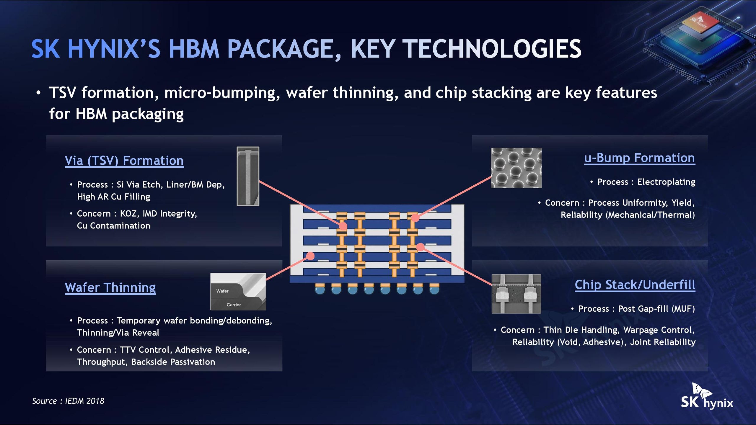
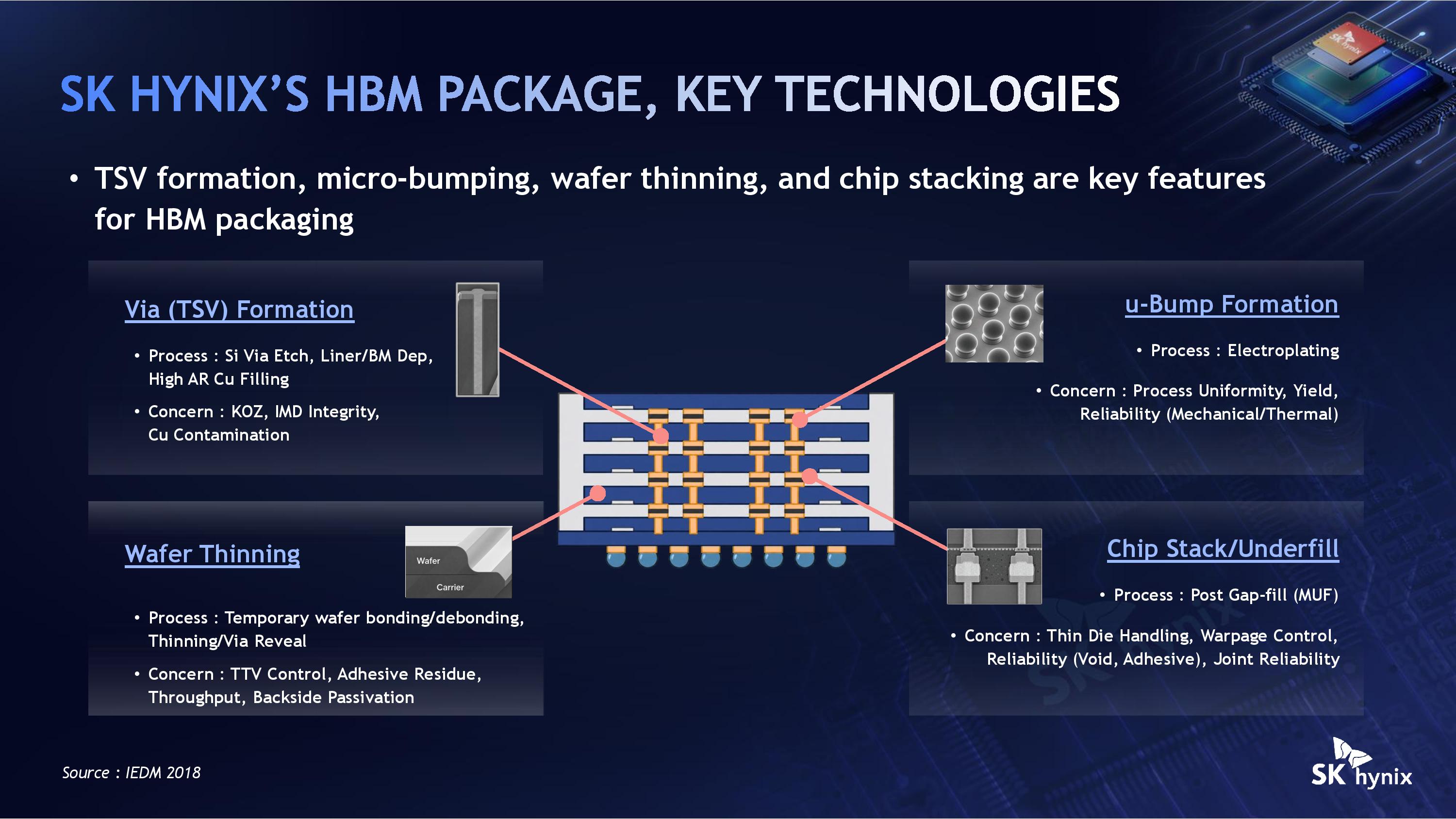
While rival memory makers like Samsung previously signaled ambitions to deploy hybrid bonding as early as HBM4, SK hynix’s continued reliance on its proprietary Advanced Mass Reflow-Molded Underfill (MR-MUF) technology demonstrates that traditional micro-bump stacking remains viable—and practically necessary—for the immediate future.
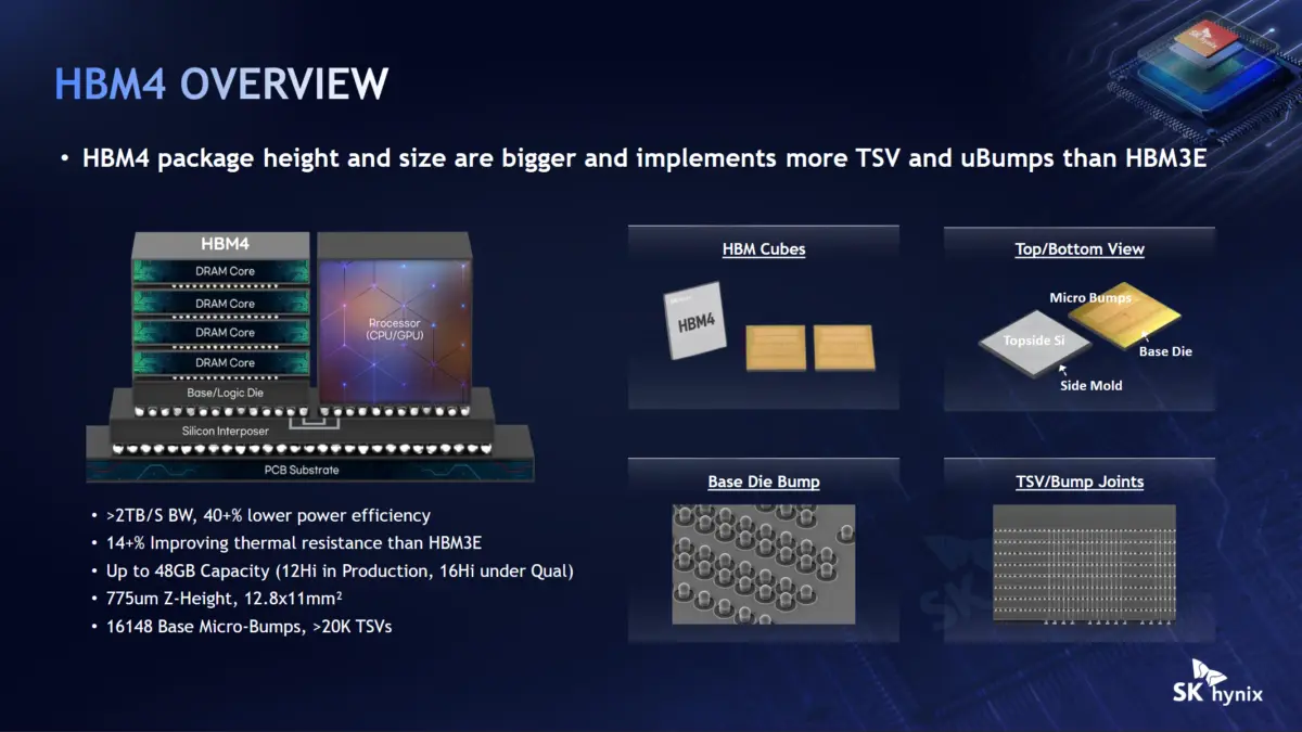
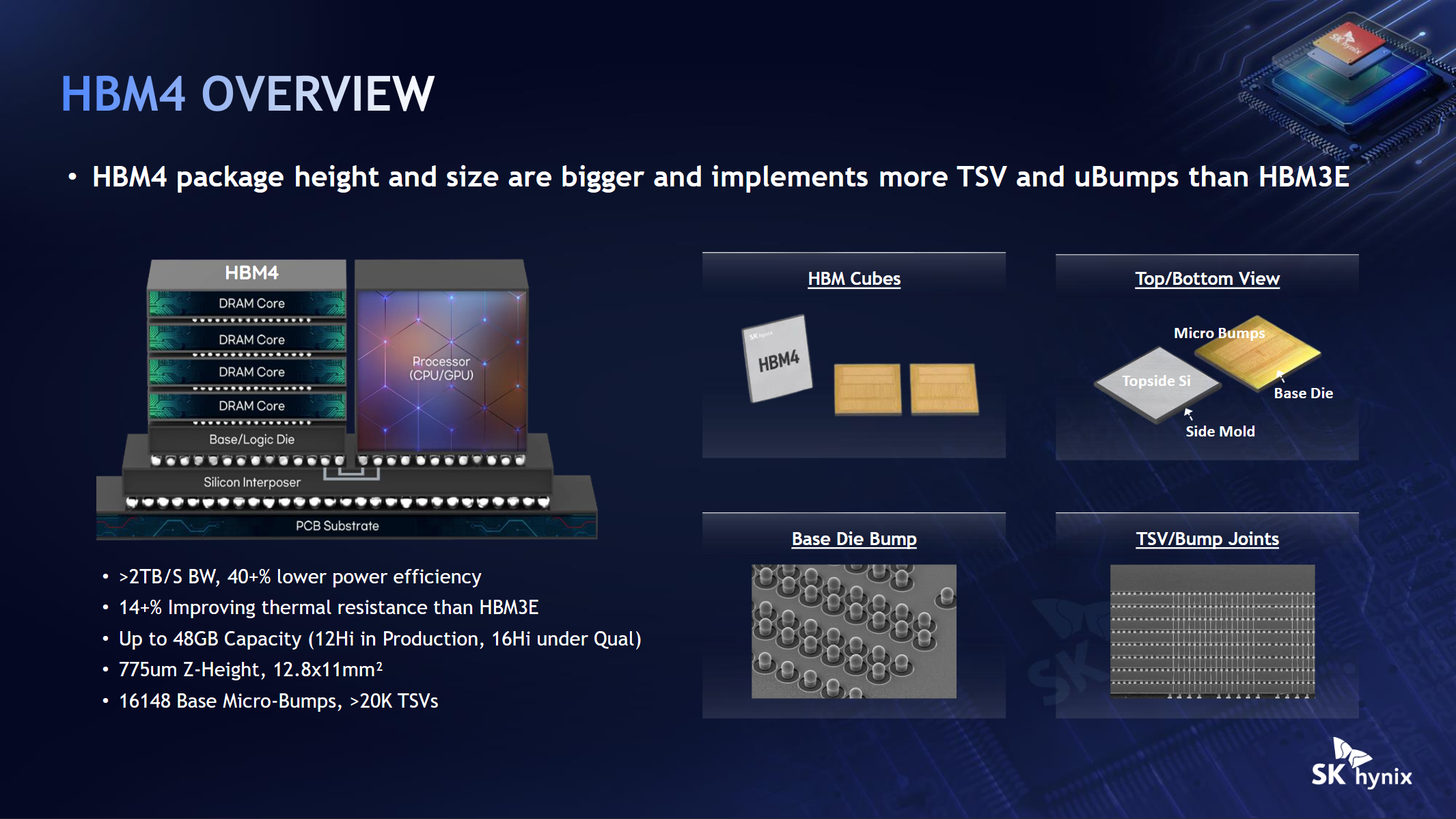
However, as AI accelerators demand denser, taller memory stacks reaching up to 16-Hi and 20-Hi configurations, the physics of stacking bare silicon are colliding with brutal thermal and mechanical limits. With package height restrictions capped strictly at 775 microns, a fierce debate is emerging over how much taller memory stacks can grow before efficiency starts to plateau.
Detailed Chronology of the HBM Packaging Transition
The path to HBM4 and beyond has been defined by a tense race between established mass-reflow techniques and revolutionary direct-bonding architectures. Understanding how the industry arrived at the current crossroads requires mapping the key technological milestones:
May 2025: Samsung publicly commits to deploying hybrid bonding for its HBM4 memory lines, raising expectations that copper-to-copper stacking would become the de facto industry standard for next-generation AI silicon. Meanwhile, SK hynix positions hybrid bonding as a secondary, long-term backup behind its proven MR-MUF process.
March 2026: Industry supply chain reports indicate that SK hynix places its first mass-production hybrid bonding tool order—a single inline system pairing Applied Materials and Besi tools valued at approximately 20 billion KRW ($15 million USD). Market researchers like Counterpoint Research project full-scale commercialization for HBM5 around 2029–2030.
Early 2026 (JEDEC Standards Update): The JEDEC Solid State Technology Association formally raises the HBM4 package thickness ceiling from the 720-micron limit that governed HBM3E to 775 microns. This crucial vertical relaxation relieves immediate manufacturing pressures, buying memory engineers extra room to scale up to 12-Hi and 16-Hi stacks without forcing an immediate, high-risk transition to hybrid bonding.
August 23, 2026 (Hot Chips 2026 Presentation): SK Hynix VP Jaesik Lee definitively rules out hybrid bonding for HBM4E during his technical presentation. He highlights the strict physical boundaries of the 775-micron limit and details the constraints surrounding the company’s newly unveiled iHBM (integrated HBM) cooling architecture.
Supporting Context & Metrics: The 775-Micron Wall and Thermal Physics
The 775-Micron Constraint
To understand why hybrid bonding has been delayed, one must understand the microscopic geometry of modern GPU and accelerator packages. When a high-performance AI processor is assembled, a cold plate must be attached directly to the top of the package. To ensure even, efficient heat transfer, both the central logic die and the surrounding memory stacks must be mechanically ground down to expose bare silicon of a uniform height.
Because standard 300mm logic wafers measure exactly 775 microns in thickness, the adjacent memory cubes cannot exceed this vertical threshold. If a memory stack grew any taller, it would "stand proud" of the processor beside it, creating uneven contact gaps that would catastrophically degrade cooler mounting and thermal dissipation.
"That’s the kind of limit that we can go up so far, because the logic wafer thickness is also 775 microns," Jaesik Lee explained during his Hot Chips session.
Shrinking Gaps and Thermal Resistance
As memory stacks evolve from 12-Hi configurations into 16-Hi HBM4 (currently shipping 48GB per cube in customer qualification) and eye future 20-Hi designs, the physical dimensions inside the package shrink drastically.
Core Die Thickness: Core DRAM dies in 16-Hi stacks are thinned down to roughly 50 microns.
Inter-Die Gap: The microscopic gap between stacked dies is halved compared to 12-Hi generations.
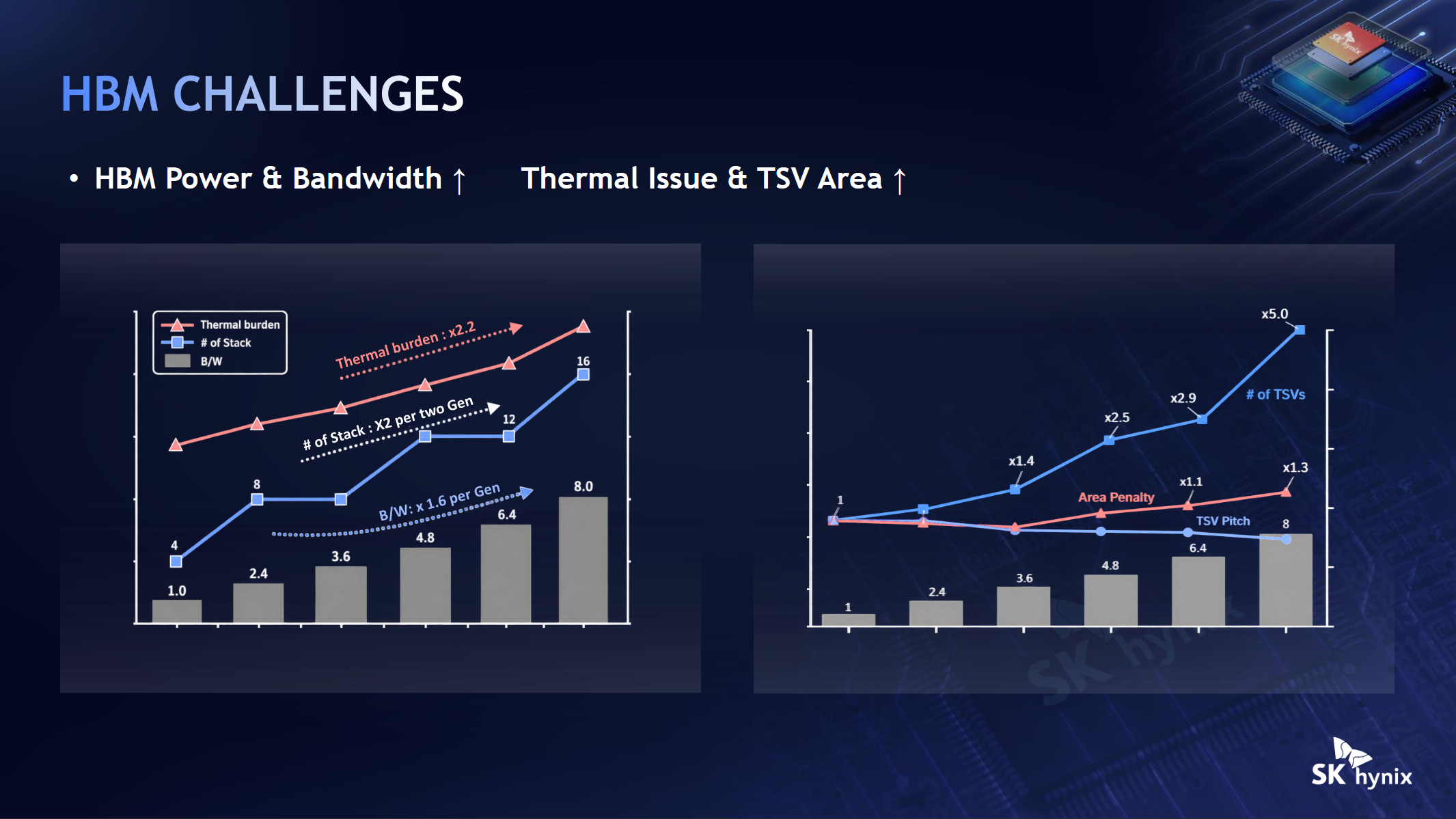
Thermal Burden: SK hynix’s internal metrics indicate that thermal burdens across successive HBM generations have multiplied by 2.2x, driven by explosive leaps in pin speeds—rising from a modest 1 Gbps in early HBM implementations to a blistering 8 Gbps to 10 Gbps in HBM4.
Thinner dies inherently leave the stack with proportionally more oxide layers, which conduct heat significantly worse than raw silicon. Furthermore, mass reflow-molded underfill (MR-MUF) struggles as gaps shrink to sub-50-micron tolerances while maintaining structural warpage control across 16 layers.
Why Hybrid Bonding is Hard
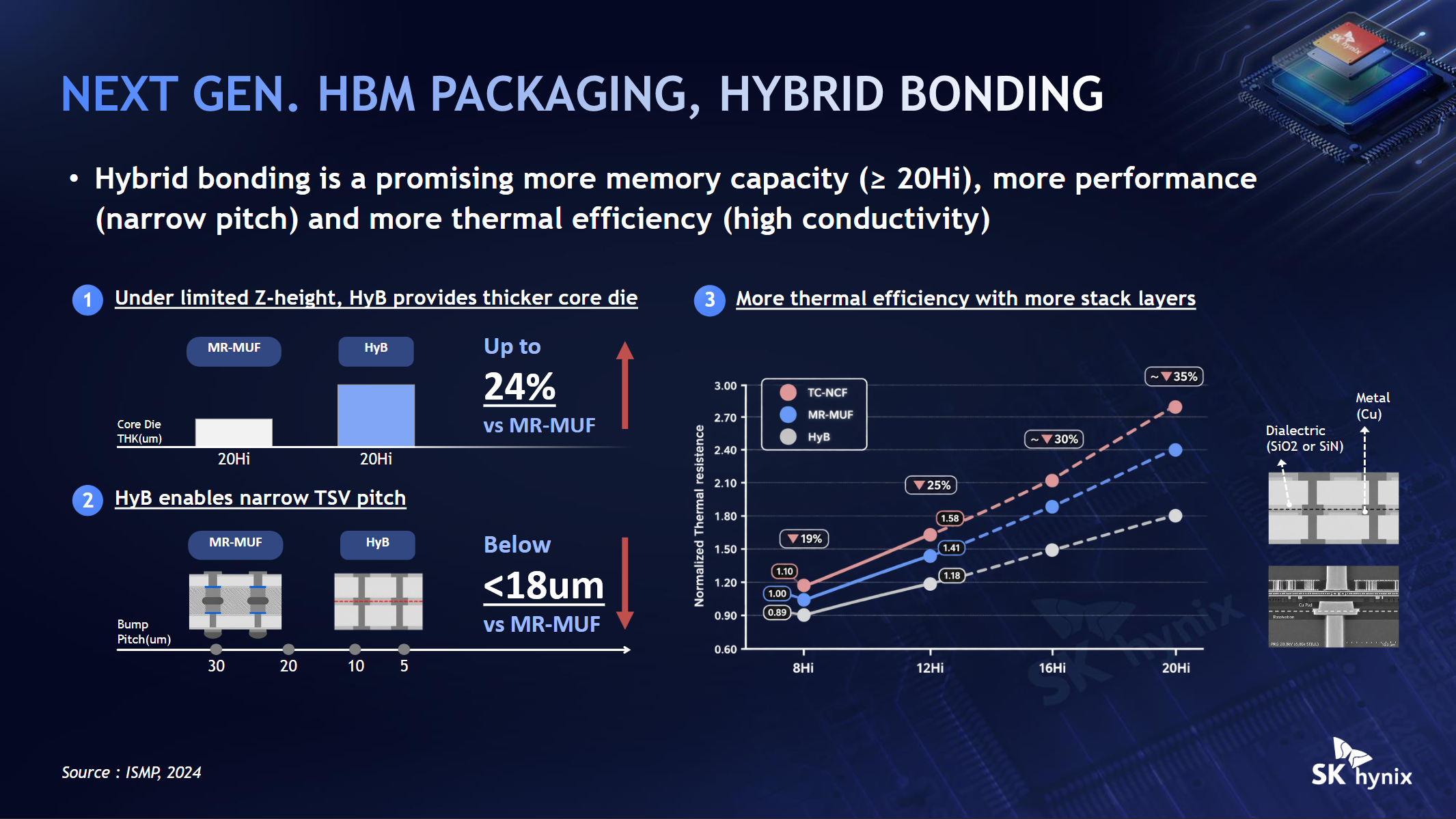
Hybrid bonding removes conventional micro-bumps entirely, utilizing flat copper pads and oxide surfaces bonded at room temperature before relying on thermal expansion during a curing cycle to lock the electrical and mechanical connection.
While successful hybrid bonding would allow core dies to grow up to 24% thicker in a 20-Hi configuration, cut thermal resistance by ~35% compared to MR-MUF, and drop bump pitch below 18 microns (versus ~30 microns for current MR-MUF), the execution is intensely complex. Bonding a single layer in a laboratory environment is vastly different from reliably aligning and fusing 16 to 20 ultra-thin layers without yield-killing defects.
Official Statements and Industry Perspectives
The discourse at Hot Chips 2026 highlighted a growing philosophical rift among memory architects regarding the physical limits of vertical stacking.
During the event’s rigorous Q&A session, Tanj Bennett of SemiAnalysis challenged the industry’s relentless push toward taller stacks, arguing that hyper-verticality ultimately dilutes raw silicon throughput. Bennett pointed out that fundamental DRAM cell-level operations yield around 20 TB/s per square centimeter, whereas a massive 20-Hi HBM stack tops out at an aggregate 4 TB/s—effectively running slower on average than standard DDR5 memory while devouring vastly more manufacturing capacity.
"As you get to 20 high, the average speed of that memory is slower than DDR5," Bennett noted. "Why is it better to be using the height of the HBM stack instead of intelligently placing cheaper memory around it?"
In response, Jaesik Lee defended the memory industry’s trajectory, emphasizing that modern training workloads demand both raw bandwidth and massive localized capacity. However, he conceded that future AI inference architectures may increasingly favor a tiered memory approach.
This hybrid memory paradigm is already taking shape in cutting-edge designs like Nvidia’s Vera Rubin platform, which intelligently pools ultra-fast HBM4 with lower-cost LPDDR5X memory over high-speed interconnects (such as NVLink-C2C). Furthermore, specialized specifications like High Bandwidth Flash (HBF)—co-developed by SK hynix and SanDisk—aim to extend similar tiering philosophies into the NAND flash domain.
The iHBM Architecture: Cooling at the Source
Addressing the escalating thermal crises within dense AI servers, SK hynix also elaborated on its iHBM (integrated HBM) thermal architecture, first teased earlier in the year.
Mechanism: iHBM embeds thermally conductive, electrically insulating blocks directly inside the base die’s die-to-die (D2D) PHY region—the exact interface hotspot where electrical power density reaches its maximum peak.
Performance Claim: SK hynix claims this approach slashes thermal resistance by more than 30%.
Design Limitations: Because these thermal blocks are physically embedded within the base die architecture, they cannot be retrofitted into existing memory generations. They require deep, synchronized co-design with the customer’s processor layout from day one. Consequently, iHBM is strictly slated for next-generation HBM5 platforms, with commercial mass production unlikely before 2028.
It joins competing vendor initiatives, such as Samsung’s Heat Path Block cooling methodology and Micron’s redesigned base-die circuits, highlighting an industry-wide scramble to solve thermal bottlenecks at the silicon root.
Future Outlook
As the artificial intelligence boom strains compute infrastructure, the memory subsystem has transformed from a commodity component into the primary architectural bottleneck of modern AI accelerators.
SK hynix’s commanding market position—holding roughly 70% of Nvidia’s HBM orders for upcoming generations—gives its roadmap massive industry weight. By pragmatically pushing hybrid bonding out to HBM5 and doubling down on refined MR-MUF methods for HBM4 and HBM4E, SK hynix is betting on manufacturing stability over premature technological leaps.
Yet, the clock is ticking. As stack heights approach 20 layers and power densities surge past the cooling capabilities of traditional packaging, the semiconductor industry must soon decide whether to force hybrid bonding into production or fundamentally reinvent how memory, logic, and cooling coexist on the silicon interposer.