

Executive Overview
The artificial intelligence boom has brought with it an unprecedented hardware crisis: the widening silicon gap between computational power and memory capacity, bandwidth, and cost. While High Bandwidth Memory (HBM) remains the undisputed king of server-grade data center accelerators, its exorbitant cost, manufacturing complexity, and constrained wafer supply have left the broader consumer, mobile, and client-device ecosystems searching for a viable alternative.
At Hot Chips 2026, Samsung stepped up to address this pressing industry bottleneck with a groundbreaking presentation detailing its newly validated LPDDR5X-PIM (Processing-in-Memory) technology. By embedding localized logic units directly into the low-power memory standard, Samsung is challenging traditional von Neumann architecture constraints. Rather than forcing data to continuously shuttle back and forth between the memory subsystem and the host processor—a primary source of latency and power consumption—LPDDR5X-PIM handles fundamental computing tasks locally, inside the DRAM banks themselves.

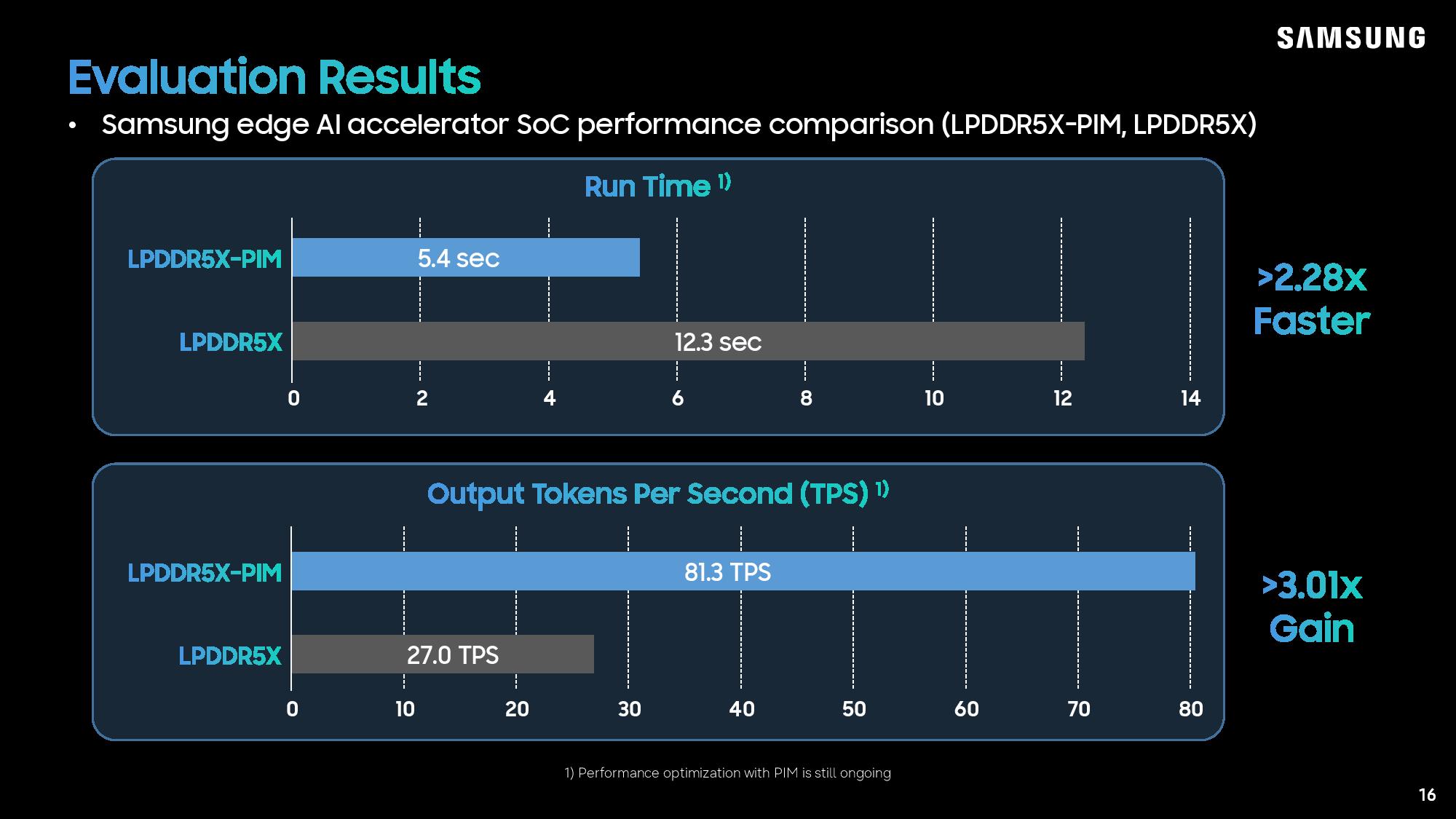
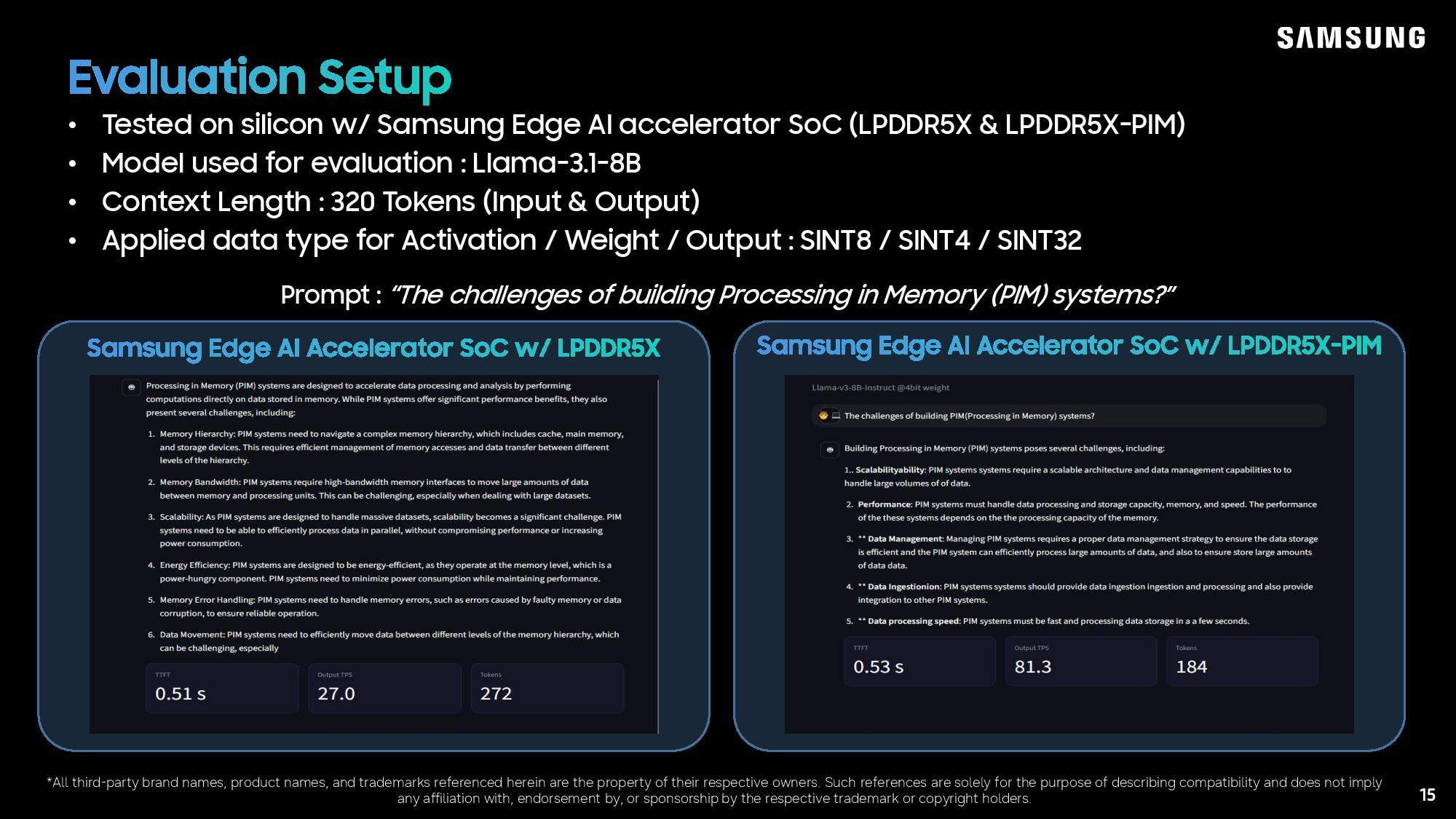
The impact of this architectural shift is dramatic. Samsung’s preliminary benchmarks reveal that LPDDR5X-PIM achieves a 2.28x speedup in model runtime and a staggering 3.01x increase in tokens per second (TPS) when running large language models (LLMs) like Llama 3.1 (8B parameters) on edge accelerators. As the industry faces soaring memory costs and rising power demands, Samsung’s innovation signals a monumental turning point for edge AI, client computing, and power-efficient server applications.
Detailed Chronology: The Evolution of Processing-in-Memory (PIM)
Samsung’s journey toward commercializing Processing-in-Memory has been deliberate, shifting from experimental academic concepts to rigorously validated, production-ready silicon standards.

2021–2023: The HBM-PIM Pioneer Phase
Samsung first introduced the concept of Processing-in-Memory to the public as early as 2021. The earliest commercial and experimental iterations of PIM were deployed through High Bandwidth Memory (HBM) stacks, famously piloted by modifying AMD MI100 accelerator GPUs.
While HBM-PIM proved the viability of in-memory arithmetic—performing basic multiply-accumulate (MAC) operations directly within the DRAM stack—it came with significant architectural compromises. Because of the dense 3D-stacked nature of HBM, engineering teams had to cut away portions of valuable memory banks to accommodate the added logic circuitry. Furthermore, as Micron and other semiconductor giants warned at Hot Chips 2026, the global demand and silicon gap for HBM wafers continue to widen exponentially, pricing out smaller accelerators and client-side devices.
Early 2026: The LPDDR5X-PIM Breakthrough
Recognizing that HBM was far too expensive and power-hungry for mobile, client, and edge computing environments, Samsung shifted its focus to the low-power DRAM ecosystem. Earlier this month, Samsung officially introduced the industry’s first LPDDR5X-PIM memory standard.
Rather than stopping at a conceptual proof-of-concept—which was initially teased back when HBM-PIM launched—Samsung arrived at Hot Chips 2026 showcasing fully validated silicon. The company also turned its gaze toward the horizon, confirming that development on LPDDR6X-PIM is already underway, with an initial specification targeted for JEDEC standardization later this year.
Architectural Mechanics: How LPDDR5X-PIM Operates
To fully appreciate Samsung’s engineering achievement, one must examine how logic was successfully integrated into LPDDR5X without sacrificing the structural integrity of the memory banks.
Dual-Mode Operation and Address Align Mode (AAM)
Samsung’s LPDDR5X-PIM is engineered to operate in two distinct modes:
- Single-Bank Mode: Functions identically to traditional, conventional DRAM, handling standard read and write instructions through conventional memory controllers.
- Multi-Bank Mode (PIM): Engages the localized PIM logic to execute parallelized arithmetic operations.
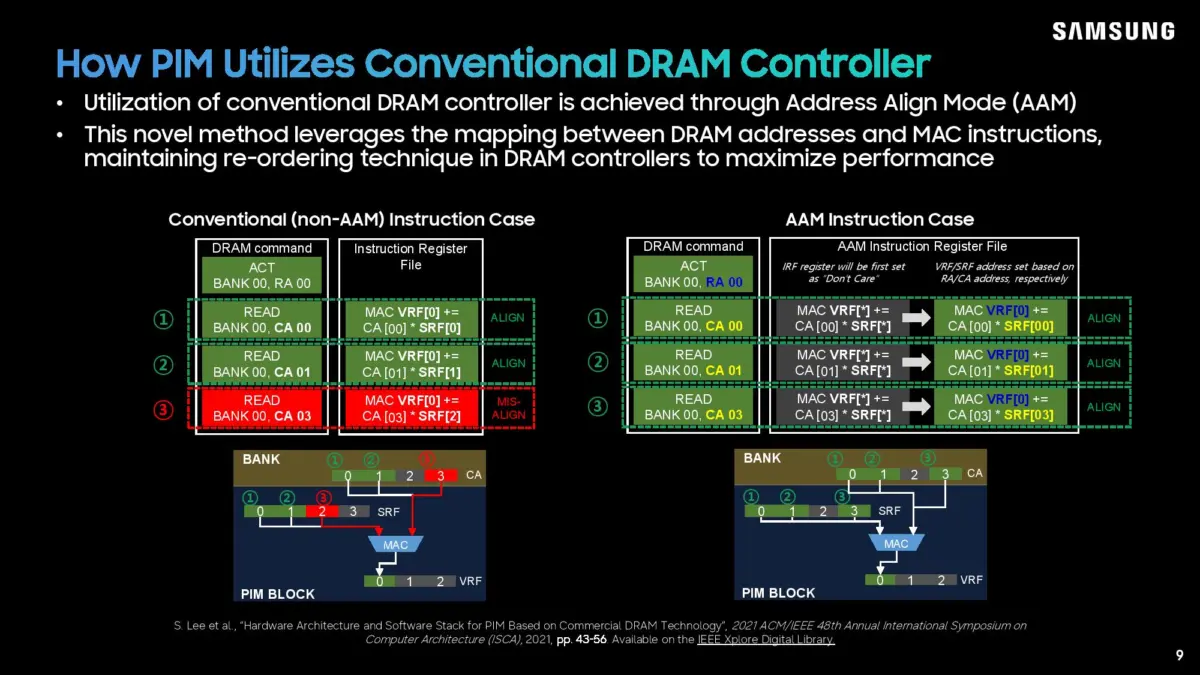
The primary engineering challenge in developing LPDDR5X-PIM was command reordering. Conventional DRAM controllers frequently reorder memory commands to optimize bus efficiency, which wreaks havoc when executing synchronous in-memory vector calculations.
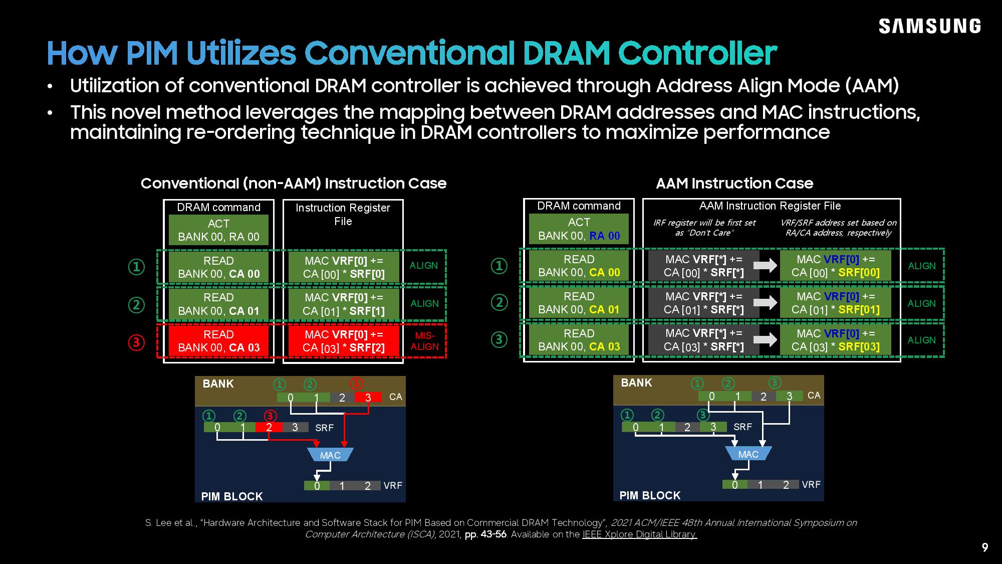
To solve this, Samsung developed Address Align Mode (AAM). Instead of relying purely on an Instruction Register File to dictate calculation schedules, AAM maps standard DRAM row addresses (RA) and column addresses (CA) directly to MAC instructions, assigning the Vector Register File (VRF) and Source Register File (SRF) addresses dynamically. This allows standard memory controllers to orchestrate complex AI operations without extensive hardware rewrites.
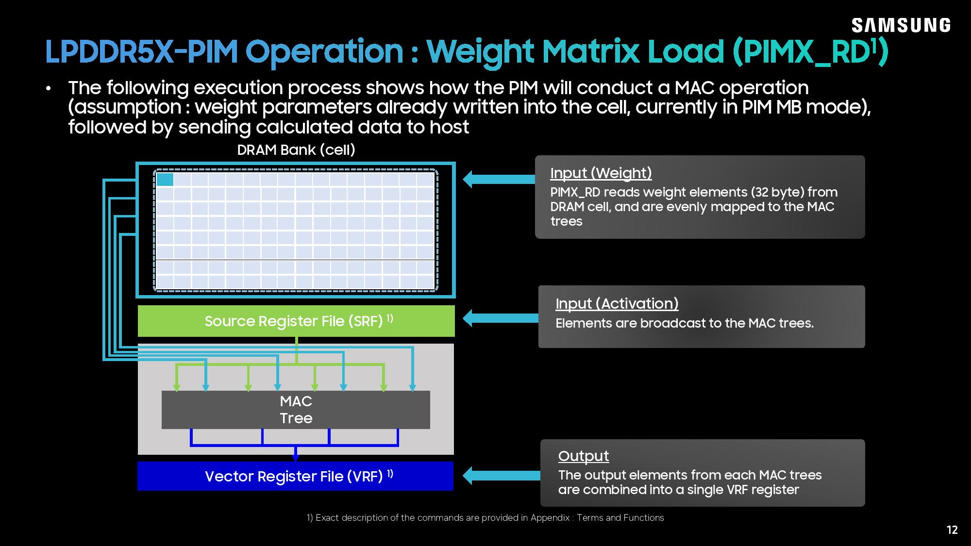
Step-by-Step Data Flow in a MAC Operation
During a typical Multiply-Accumulate (MAC) operation—assuming weight parameters are pre-loaded into the memory cells—data moves through the silicon in a highly optimized pipeline:
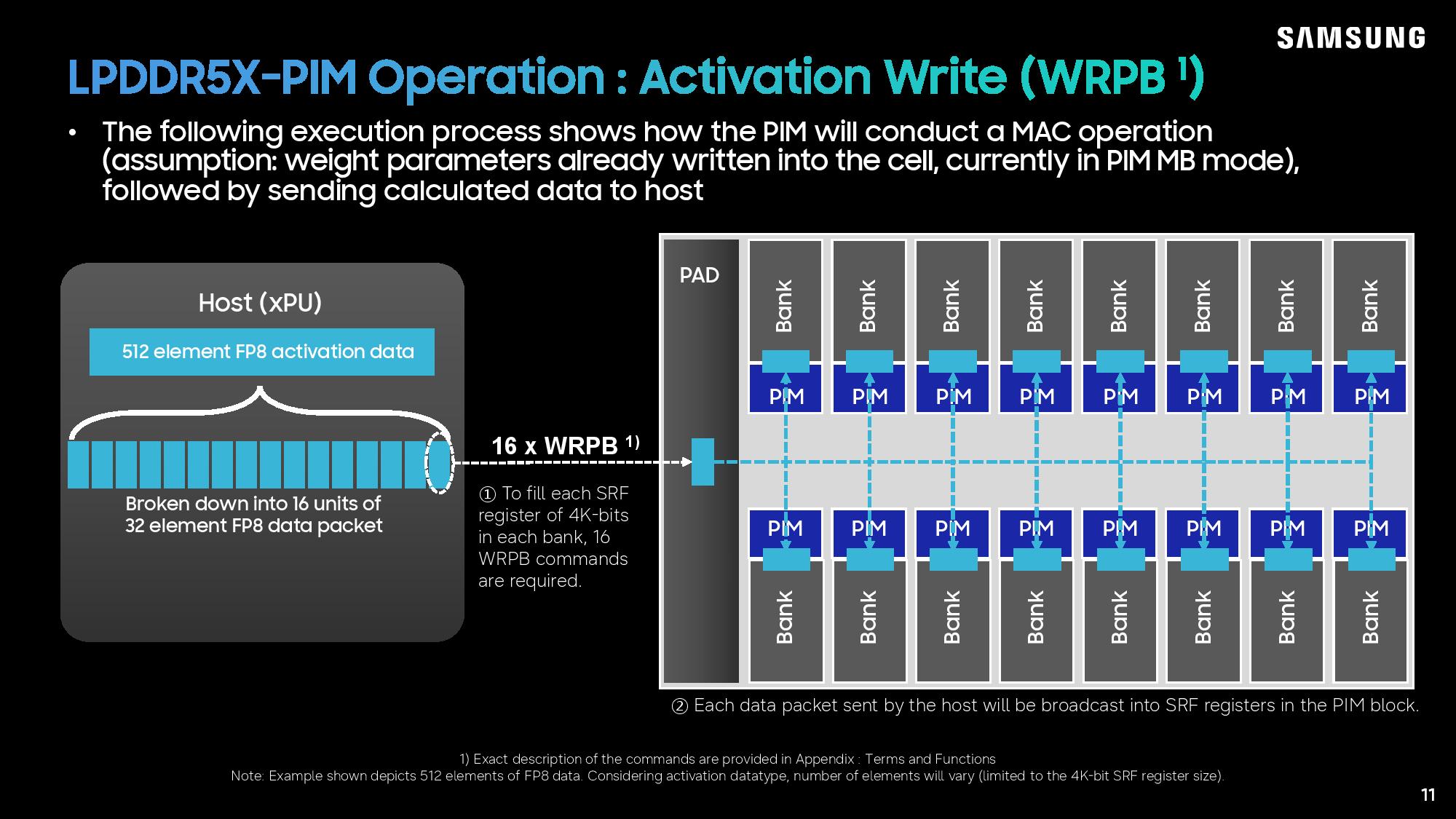
- Activation Loading: 512 bytes of FP8 activation data are segmented into sixteen 256-bit packets, which are written directly into the memory banks and cataloged within the Source Register File (SRF).
- Execution: A specialized
PIMX_RDcommand reads the weight data out of the DRAM bank, routing it directly into parallel MAC trees alongside the activation data waiting in the SRF. - Vector Registration: Once the integer or floating-point calculations are finalized, the resulting output vector from each operation is written into the Vector Register File (VRF), which boasts a size of 1 kbit (accommodating up to four concurrent calculations).
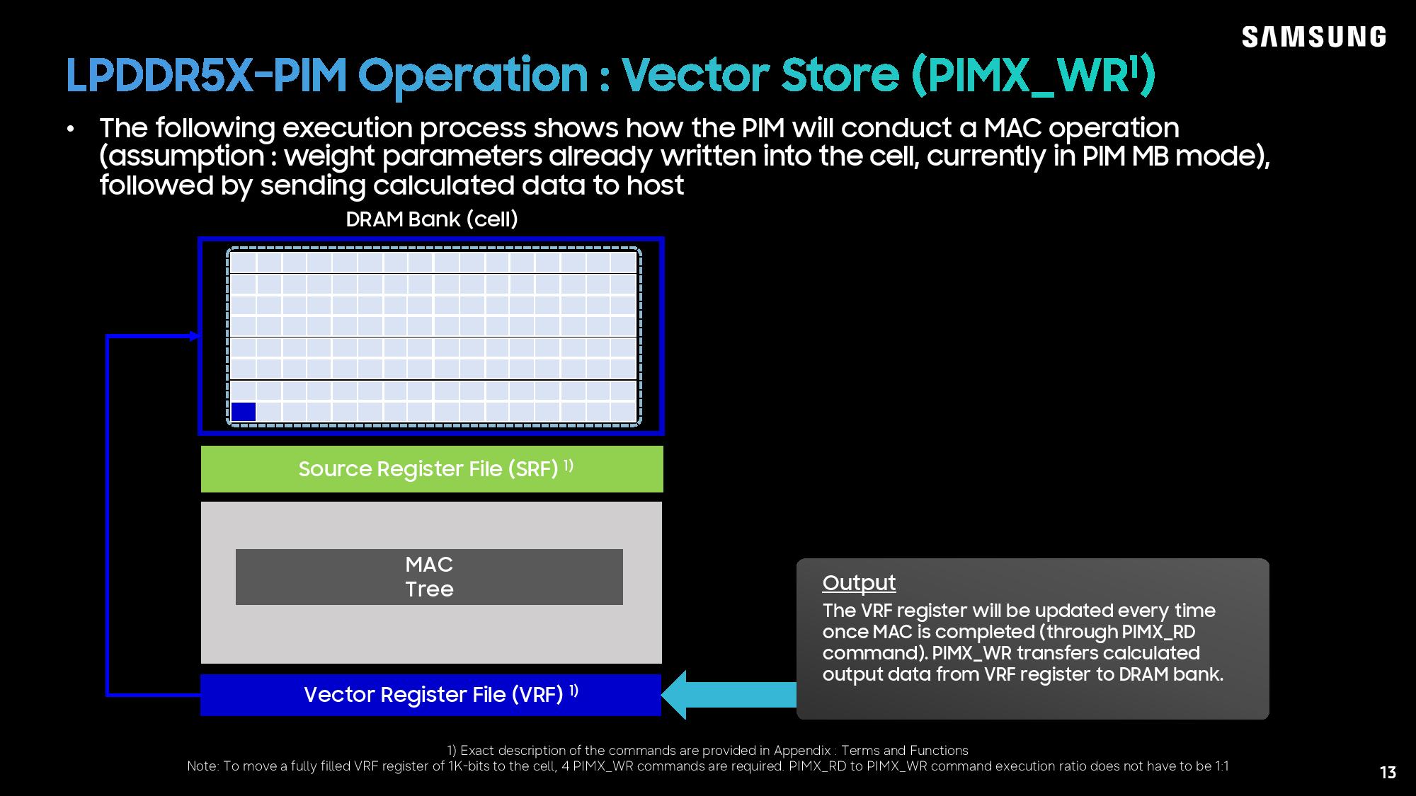
- Writeback: A
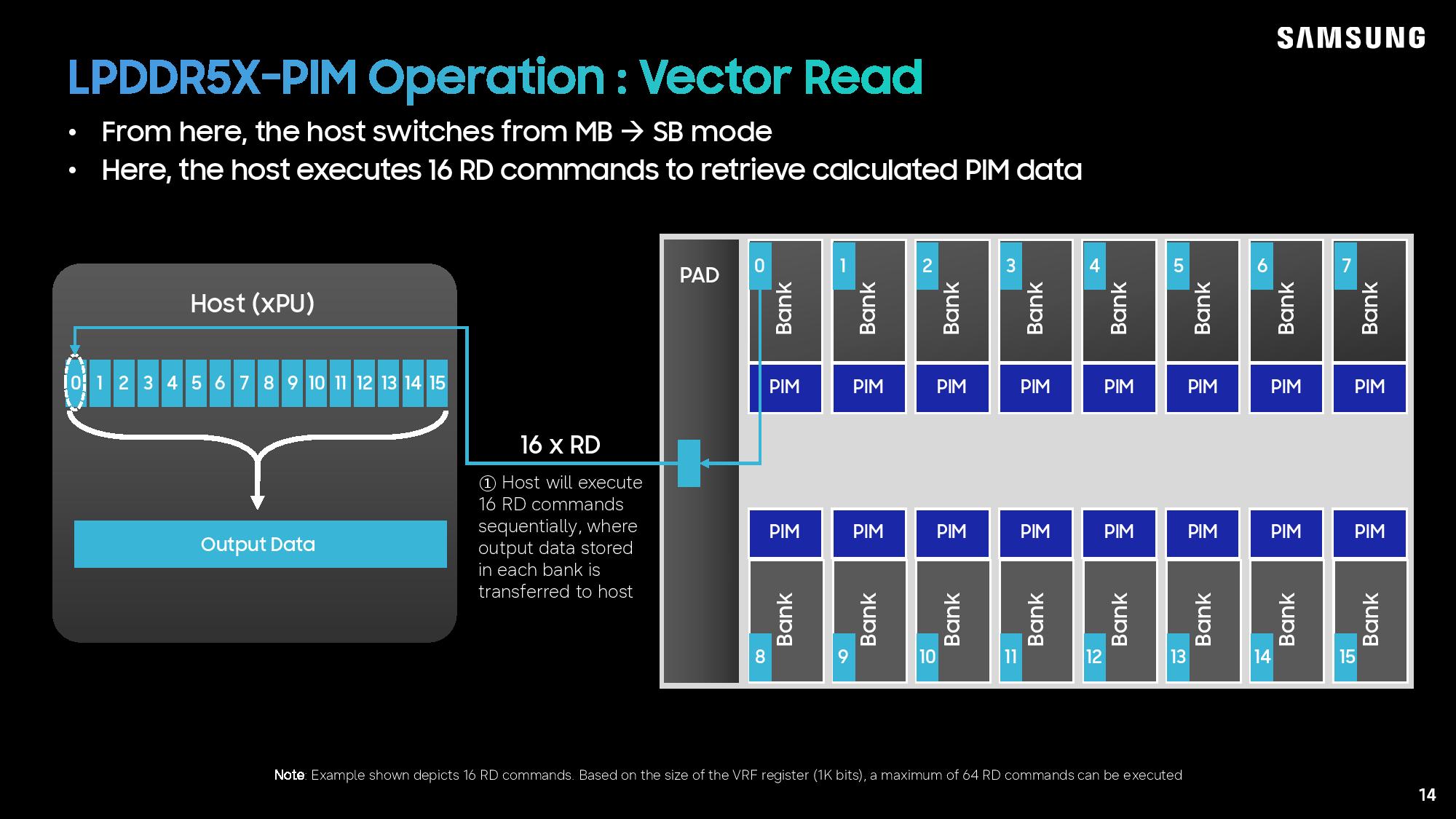
PIMX_WRcommand transfers the processed output data back into the DRAM bank. - Host Retrieval: Finally, the host processor switches the memory back to single-bank (conventional DRAM) mode and executes a series of reads to gather the finalized outputs from the memory banks.
Supporting Context & Metrics: Specs and Performance
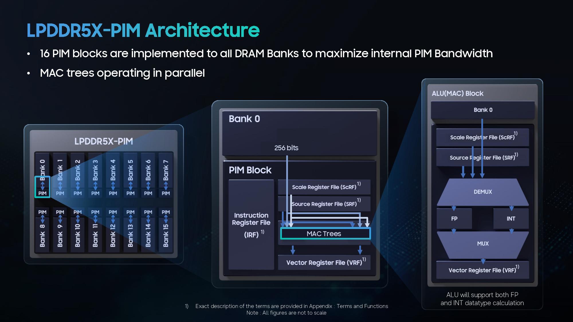
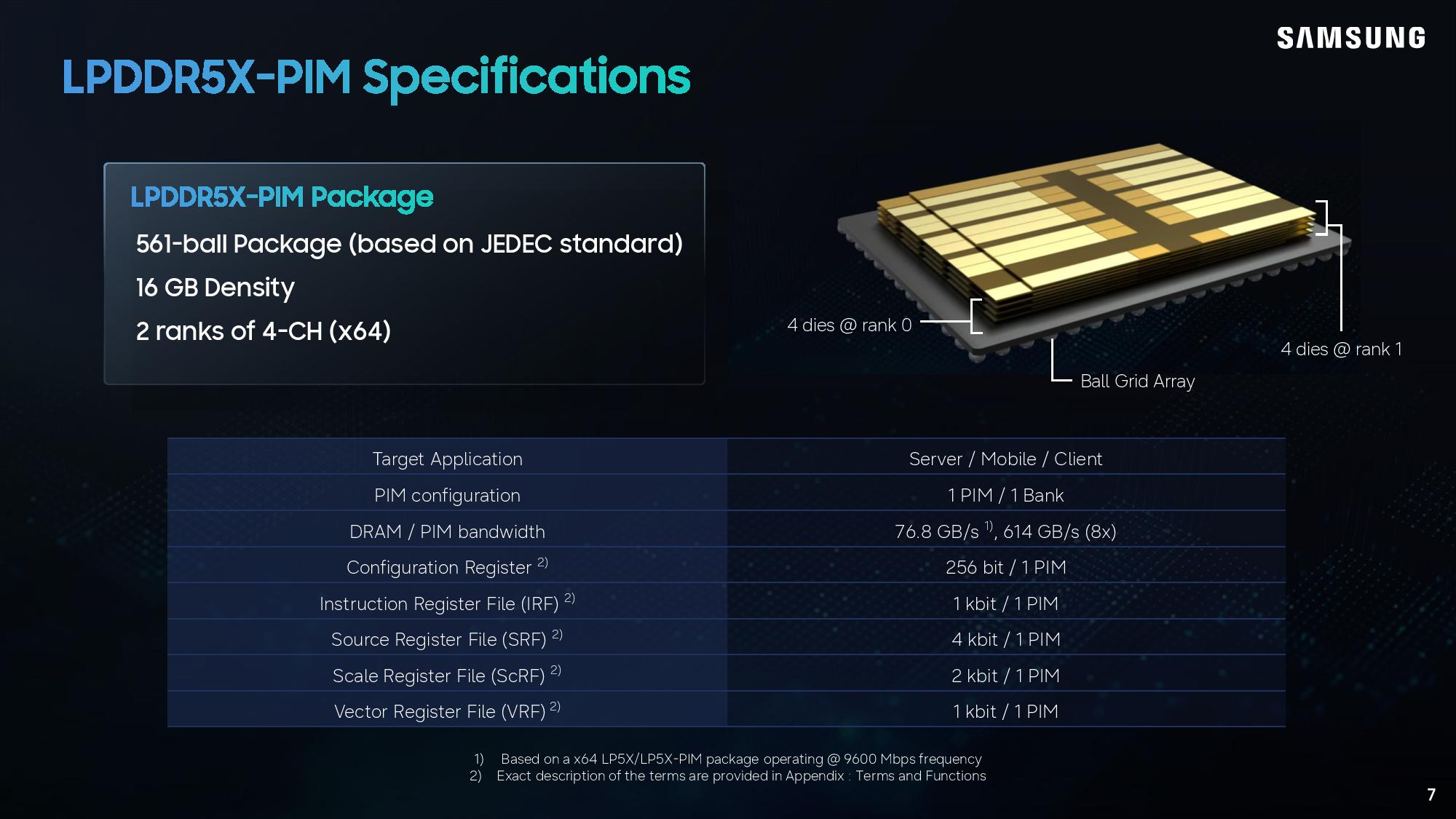
Samsung’s LPDDR5X-PIM maintains a physical footprint strikingly similar to standard LPDDR5X, utilizing a conventional 561-ball array packaging grid. The physical module consists of two 64-bit ranks built across eight total dies (four dies per rank), housing 16 GB of capacity.
| Metric / Specification | Standard LPDDR5X-9600 | LPDDR5X-PIM |
|---|---|---|
| Peak Memory Bandwidth | 76.8 GB/s | 614 GB/s (8x increase via local logic) |
| Model Runtime Performance | Baseline | 2.28x Improvement |
| Throughput (Tokens per Second) | Baseline | 3.01x Increase |
| Supported Data Formats | Standard Integers / Floats | FP8, Integer, and Floating-Point |
| Target Architecture | Host-Bound Computing | Processing-in-Memory (PIM) |
Analyzing the Performance Gains
In preliminary benchmarks leveraging an edge AI accelerator testing the Llama 3.1 model (8 billion parameters), Samsung demonstrated staggering performance uplifts. Model runtime saw a 2.28x improvement, while token generation surged by 3.01x.
Some industry attendees at Hot Chips raised questions regarding slight output variations observed during early testing. Samsung addressed these concerns directly, explaining that software and compiler optimizations are ongoing to ensure bit-exact mathematical precision, though the core hardware performance multipliers are expected to remain firmly intact.
Official Statements and Power Consumption Realities
One of the most paradoxical challenges of integrating computing logic into a "low-power" memory standard like LPDDR5X is thermal and electrical management. By definition, adding arithmetic logic units (ALUs) and MAC trees to DRAM increases active silicon real estate.
However, Samsung’s engineers insist that overall power consumption will actually decrease relative to traditional von Neumann architectures. During his presentation, Samsung presenter Karam Hwang clarified the distinction between peak and average power draw:
"We’re not having a significant power increase overall. While peak power consumption will be much higher due to the bursty nature of PIM workloads, the system saves an immense amount of energy by drastically reducing the number of times data must physically shuttle back and forth across the memory bus to the host processor."
By eliminating the energy-intensive data transfer bottleneck between the CPU/NPU and the memory chips, the thermal and electrical toll of moving heavy AI weights is effectively neutralized.
Future Outlook: Expanding Beyond Mobile
Historically, LPDDR memory standards have been strictly confined to smartphones, tablets, and ultra-thin laptops. However, the hardware landscape is shifting rapidly.
Recent architectural developments—such as Nvidia adopting LPDDR5X for its Vera CPU via serviceable SOCAMM2 modules, and Intel pairing LPDDR5X with its newly unveiled "Crescent Island" AI accelerator—prove that low-power memory is graduating to enterprise and server spaces.
Samsung’s strategic roadmap targets three primary verticals: servers, client PCs, and mobile devices. By bringing LPDDR5X-PIM to market, Samsung is empowering edge AI applications on local devices while providing data centers and enterprise edge servers with a cost-effective, high-bandwidth alternative to prohibitively expensive HBM solutions.
As JEDEC prepares to draft initial specifications for LPDDR6X-PIM later this year, Processing-in-Memory is rapidly transitioning from an experimental academic curiosity into the indispensable foundation of next-generation computing architecture.
