

Executive Overview
At the Hot Chips 2026 conference, Nvidia officially showcased its next-generation hardware architecture born from its controversial $20 billion partnership with Groq. In a striking presentation, Igor Arsovski—formerly Groq’s chief architect and now Nvidia’s Vice President of Hardware—took the stage to present Groq’s proprietary inference silicon integrated under the Nvidia banner. Dubbed the Groq 3 LPX rack, this ultra-fast hardware solution relies on the LP30 chip, which abandons traditional High Bandwidth Memory (HBM) entirely in favor of an exclusive, high-speed on-die SRAM layout.
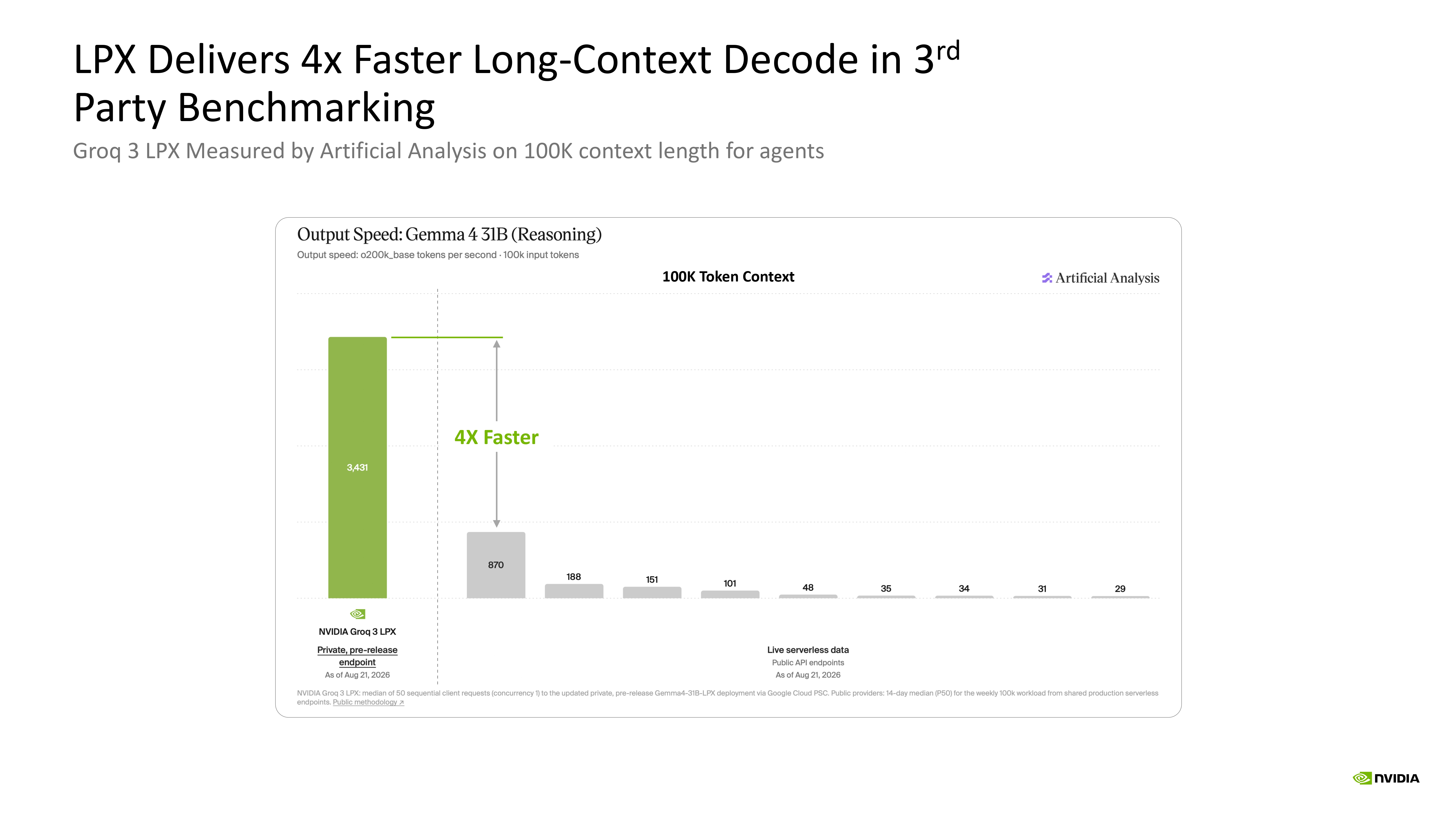
The architecture is designed to target the single largest bottleneck in modern generative AI deployments: the memory-access latency that plagues single-token generation (decode phase). By maintaining model weights natively within ultra-low-latency SRAM, the system achieves unprecedented throughput. Third-party testing conducted by Artificial Analysis revealed that a 256-chip LPX rack handling a 100K-context Gemma 4 31B reasoning workload posted a staggering 3,431 output tokens per second—roughly four times faster than the next-fastest public production endpoint available on the market.
This breakthrough architecture has already reshaped Nvidia’s long-term product roadmap. Most notably, it forced the cancellation and removal of the Rubin CPX accelerators. Instead, Nvidia has positioned the LPU (Language Processing Unit) as a specialized, high-performance decode co-processor designed to work in tandem with the forthcoming Vera Rubin NVL72 platform. While this SRAM-centric approach yields unmatched generation speeds, it introduces capacity constraints that require careful integration with traditional GPU infrastructure. Furthermore, the massive commercial and technical alignment between Nvidia and Groq continues to draw intense scrutiny from antitrust regulators and lawmakers concerned with consolidation in the AI hardware ecosystem.

Detailed Chronology: From Independent Rivalry to Silicon Integration
The Genesis of the Tensor Streaming Processor
The lineage of Nvidia’s new LPU traces back to foundational architectures conceptualized by Jonathan Ross, an ex-Google TPU engineer who founded Groq. In a landmark 2020 paper presented at ISCA titled Think Fast, Groq introduced the Tensor Streaming Processor (TSP). This design rejected traditional CPU/GPU paradigms—such as complex multi-level caches, branch prediction units, and out-of-order execution—in favor of a fully deterministic, compiler-scheduled pipeline.
For years, Groq positioned its LPUs as high-performance accelerators built specifically for linear algebra workloads, operating entirely in SRAM without the latency penalties associated with external HBM stacks. However, despite technical prowess, the company faced significant capital hurdles in scaling manufacturing and software ecosystems to compete directly against Nvidia’s omnipresent CUDA framework.
The $20 Billion Strategic Alignment (December 2025)
The trajectory of the AI hardware market shifted dramatically in December 2025 when Nvidia secured a monumental $20 billion deal with Groq. Rather than an outright acquisition—a maneuver explicitly structured to sidestep immediate, formal merger reviews by federal antitrust regulators—the agreement was formalized as a massive, non-exclusive intellectual property (IP) license.

Crucially, the arrangement included the large-scale absorption of Groq’s top engineering talent, including founder Jonathan Ross and President Sunny Madra, who integrated directly into Nvidia’s hardware divisions. This high-stakes maneuver immediately reverberated through the semiconductor landscape, rendering redundant several internal Nvidia projects. At GTC 2026, Nvidia executive Ian Buck confirmed that the company had officially purged the Rubin CPX accelerators from its master roadmap, pivoting full corporate weight behind the newly acquired Groq-derived LPU technology.
The Hot Chips 2026 Reveal
The culmination of this rapid integration materialized at Hot Chips 2026. In an ironic twist of industry dynamics, Igor Arsovski walked onto the auditorium stage to present his former team’s silicon, now fully rebranded and manufactured under Nvidia’s enterprise umbrella. Opening his address with what he described as a "pinch-me moment," Arsovski walked the audience through the architectural specifications of the Groq 3 LPX rack, simultaneously publishing the industry’s first independent third-party benchmarks for the hardware.
Supporting Context & Technical Metrics
SRAM vs. HBM: The Architectural Trade-Off
The core engineering philosophy of the LP30 chip centers on eliminating external memory bottlenecks. Traditional AI accelerators rely heavily on HBM4 to store massive model weights. While HBM offers immense storage capacity, it introduces inevitable memory-access latency during the decoding phase of large language models (LLMs), where tokens are generated sequentially.
Traditional GPU Pipeline (HBM-Dependent):
[ Compute Engine ] <--- (High Latency / Bottleneck) ---> [ External HBM Stack ]

Nvidia/Groq LPU Pipeline (SRAM-Resident):
[ Deterministic Compiler-Scheduled Pipeline ] <---> [ 500MB On-Die SRAM (Zero-Latency) ]
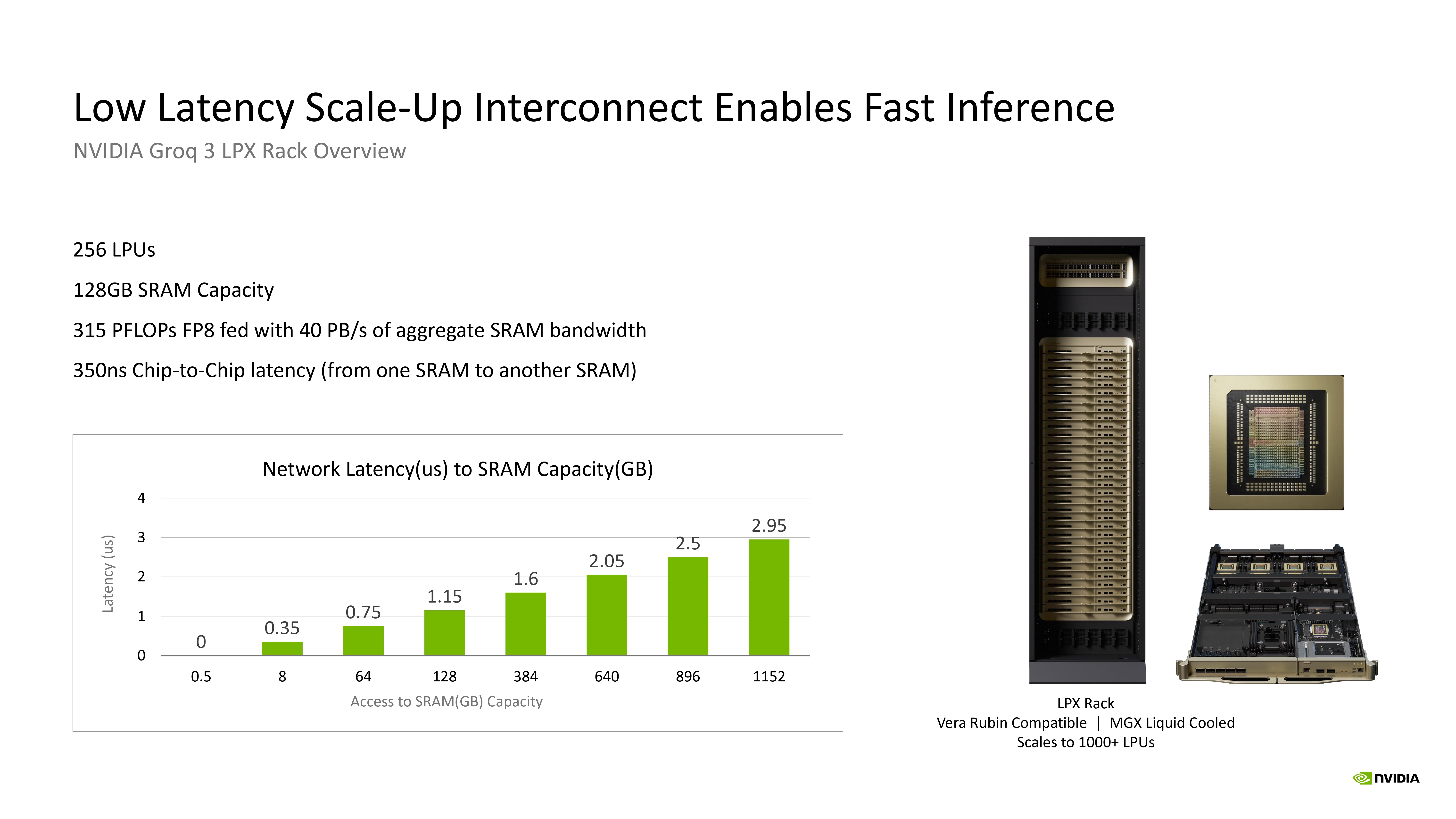
Each individual LP30 chip carries approximately 500MB of on-die SRAM and completely lacks HBM. Scaling this up to a full enterprise-grade LPX rack consisting of 256 interconnected chips yields:
- Total Memory Capacity: 128 GB of aggregate SRAM.
- Aggregate Bandwidth: 40 Petabytes per second (PB/s).
- FP8 Compute Performance: 315 PFLOPS.
- Chip-to-Chip Latency: 350 nanoseconds within a Vera Rubin-compatible, liquid-cooled MGX rack architecture capable of scaling past 1,000 LPUs.
The Cost of Capacity: Why LPUs are Co-Processors
The primary trade-off of an SRAM-only memory architecture is storage density. For comparison, a next-generation Rubin GPU accommodates 288GB of HBM4—roughly 576 times the capacity of a single LP30 chip.
Consequently, running a dense 31-billion-parameter model at FP8 precision requires distributing weights across approximately 62 LPUs. For trillion-parameter Mixture-of-Experts (MoE) models, memory constraints demand thousands of LPU chips spanning multiple racks. Recognizing this limitation, Nvidia explicitly positions the LPU not as a standalone, general-purpose replacement for its flagship GPUs, but as a dedicated high-speed decode engine.
Deterministic Execution and Power Management
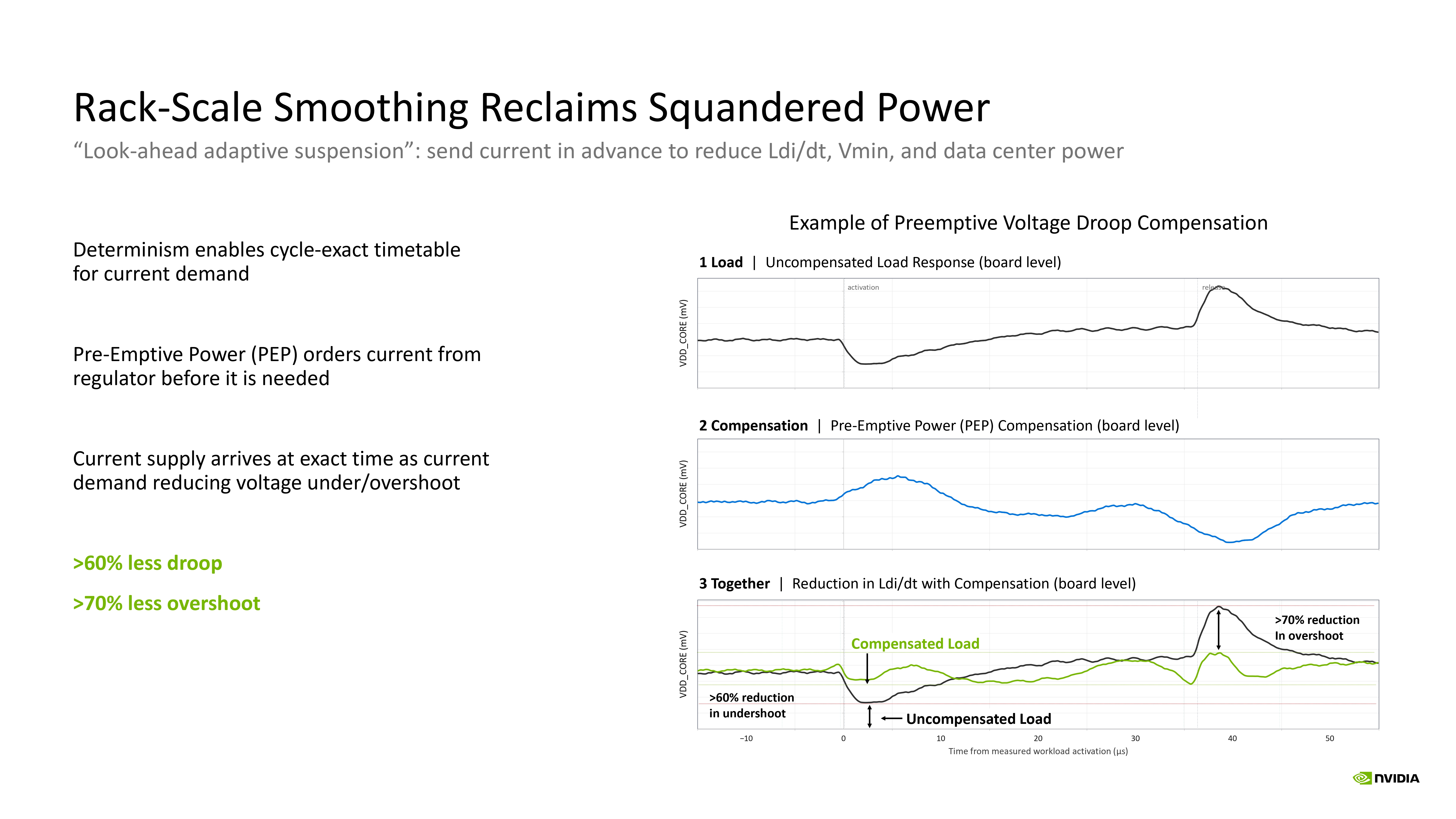
By dropping out-of-order execution and instruction caches, the LPU relies entirely on a deterministic software compiler that schedules every operation down to the individual clock cycle. This predictability yields two massive operational advantages:
- Dynamic Power Control: Because the compiler knows exact workloads cycles in advance, the hardware can pre-order current from the rack’s voltage regulators ahead of demand. This predictive regulation reduces voltage droop by over 60% and overshoot by over 70% compared to uncompensated legacy loads.
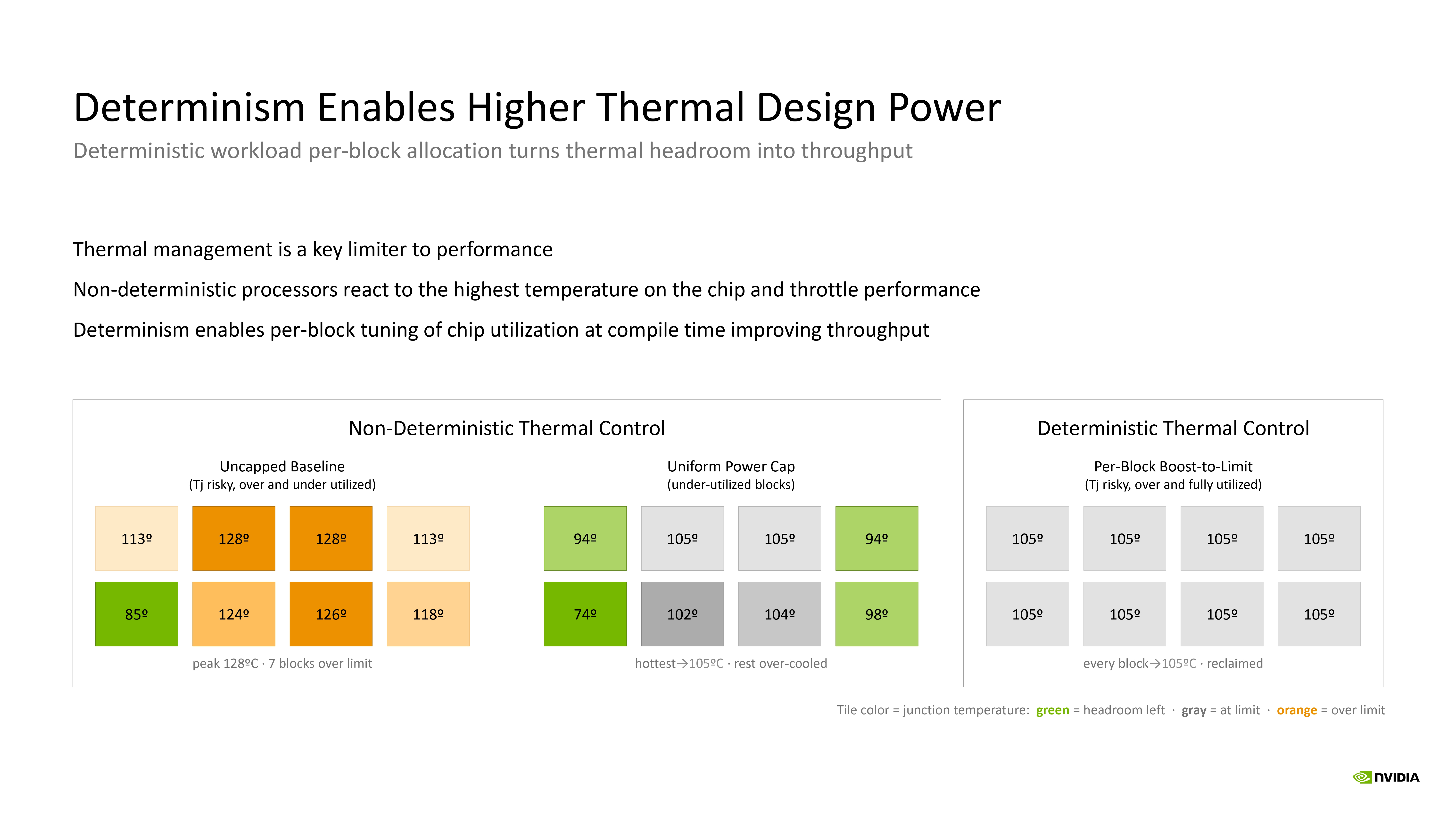
- Thermal Equalization: Deterministic scheduling allows the runtime to actively balance computational heat dissipation across the silicon grid, preventing localized hot spots. According to Arsovski, this thermal management yields an additional 10% to 11% performance uplift under fixed thermal design power (TDP) limits.
Official Statements & Industry Reception
The debut of the LPX architecture triggered widespread industry analysis regarding the future division of labor in hyperscale data centers. During the conference sessions and subsequent Q&A panels, Nvidia executives detailed how the LPU interfaces with the broader ecosystem.
Addressing concerns regarding system resilience and fault tolerance, Arsovski addressed what happens when a chip fails mid-workload within a synchronized cluster:
"Users would experience the exact same as any other hardware in the industry… you would just checkpoint it or reconfigure the hardware."
The Competitive Landscape: Cerebras CS4
Nvidia is not alone in pursuing wafer-scale or ultra-wide SRAM memory paradigms for inference acceleration. During the same Hot Chips session, rival system architect Jean-Philippe Fricker of Cerebras presented the Cerebras CS4 wafer-scale system.
Fricker asserted that the CS4 platform operates up to 30 times faster than conventional GPUs, doubling the token generation rate of the previous CS3 generation while offering ten times the token capacity. Utilizing a modular platform called "Nexus," the CS4 achieves an astonishing 43 PB/s of memory bandwidth—a figure Cerebras claims is "2,000 times higher memory bandwidth than Nvidia’s next-generation Rubin chip." Notably, Cerebras has pursued a similar strategic division of labor, having partnered with AMD in July to pair Helios GPUs for the heavy prefill phase with wafer-scale engines handling the decode phase.
Antitrust Scrutiny
The financial and structural mechanics of Nvidia’s $20 billion arrangement with Groq continue to attract intense regulatory scrutiny. In early 2026, U.S. Senators Elizabeth Warren and Richard Blumenthal formally petitioned the Federal Trade Commission (FTC) and Nvidia leadership, arguing that the transaction effectively amounted to an acquisition of Groq "in all but name" designed specifically to circumvent Hart-Scott-Rodino antitrust reporting thresholds. While no formal, deal-specific federal enforcement action had been publicly confirmed by late August 2026, the arrangement remains a focal point for lawmakers monitoring anticompetitive consolidation within the generative AI supply chain.
Future Outlook: Splitting Inference with Rubin NVL72
The commercial viability of Nvidia’s new hardware strategy hinges on its ability to seamlessly integrate LPUs with its dominant GPU ecosystem. Nvidia has outlined three primary operational topologies to split the inference workload between Vera Rubin GPUs and Groq LPUs:
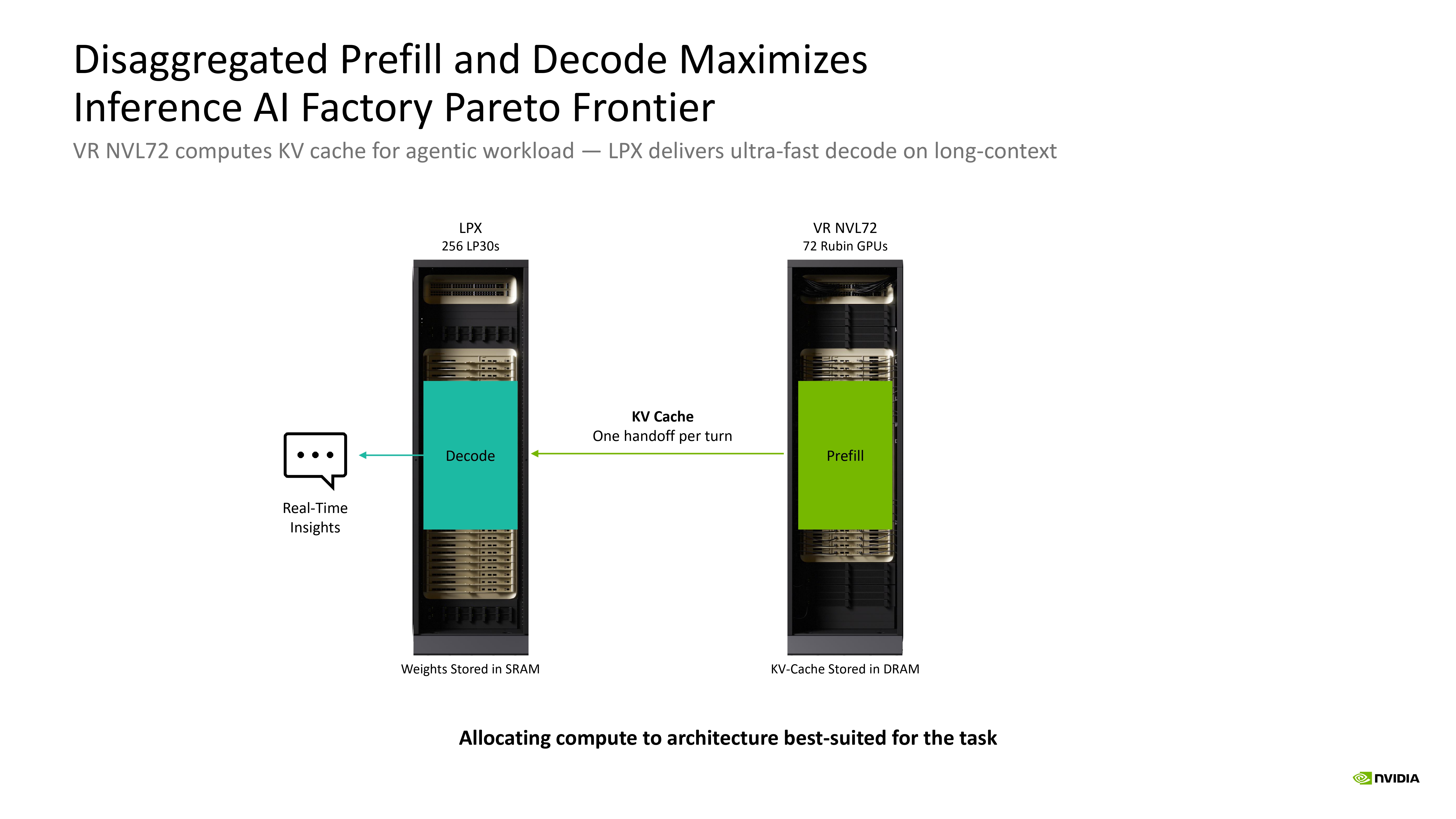
- Disaggregated Prefill and Decode: Vera Rubin GPUs handle the computationally intensive prefill phase (processing long input prompts and building the Key-Value cache), while the LPUs take over the sequential decode phase to generate output tokens at blistering speeds.
- Attention-FFN Disaggregation: The system maintains attention mechanisms and their associated caches within GPU HBM, while offloading the feed-forward network (FFN) layers directly to the LPU.
- External-Draft Speculative Decoding: A smaller, highly optimized model running on the LPU proposes speculative token sequences. The primary GPU cluster then verifies these tokens in parallel, drastically reducing overall latency over the interconnect fabric.
An FPGA-based bridge acts as the translator between the synchronous LPU domain and the asynchronous host I/O and GPU hand-off layers, orchestrated via Nvidia’s Dynamo runtime and a specialized LPU extension to CUDA. Internal benchmarks published by Nvidia indicate that these disaggregated modes deliver a three-to-five-fold performance multiplier over a pure Rubin GPU deployment on massive, two-trillion-parameter workloads featuring 400K-token cached contexts.
As hyperscalers and enterprise data centers transition toward ultra-long context windows and reasoning-heavy AI agents, the demand for deterministic, SRAM-backed generation will only intensify. Whether Nvidia’s integrated LPU-GPU hybrid approach becomes the definitive industry standard—or whether alternative architectures like Cerebras’s wafer-scale Nexus platform capture significant market share—will depend heavily on software maturity, enterprise deployment costs, and the ultimate outcome of ongoing regulatory investigations.
