

Executive Overview
Modern artificial intelligence is suffocating under its own weight. As neural networks swell from millions of parameters to hundreds of billions, the physical infrastructure supporting them is beginning to buckle. The primary culprit is not a lack of computational power, but a fundamental logistics crisis: the physical movement of data between memory storage and processing units.
In traditional computing architectures, processors feature a limited amount of high-speed static RAM (SRAM), but the bulk of an AI model’s parameters must reside in dynamic RAM (DRAM). Shuffling this mountain of data back and forth across conventional copper wires and metal interconnects creates a massive energy drain and a severe bandwidth bottleneck. When scaled across energy-hungry data centers, self-driving vehicles, and autonomous edge devices like industrial robots, these electrical limitations threaten to stall the next generation of ambient intelligence.
Enter a radical solution from a team of researchers at Cornell Tech in New York City. Recently unveiled at the IEEE/JSAP Symposium on VLSI Technology & Circuits in Honolulu, a novel optical receiver design bypasses electrical wiring altogether, using beams of light to directly program and update an AI processor’s memory on the fly.
Developed by postdoctoral researcher Yifan He and Associate Professor Jae-sun Seo, this technology uses rapid flashes of light—resembling dynamic QR codes—to alter binary memory states via photocurrents directly. By eliminating the power-hungry analog circuits that traditionally plague optical communication systems, this fully digital approach promises to dramatically shrink the energy footprint of AI memory updates. While significant hurdles remain before commercialization, the implications for robotics, automated warehouses, and resource-constrained edge devices could fundamentally transform how machines learn, adapt, and operate in the physical world.
Detailed Chronology: From Lab Bench Breakthrough to VLSI Symposium
The genesis of this optical memory-updating technique can be traced back to the growing pains of modern semiconductor design. For years, computer engineers have wrestled with the physical limitations of Moore’s Law and the widening performance gap between processing logic and memory storage—a phenomenon long known in computer architecture as the "memory wall."
The Lab Bench Demonstration
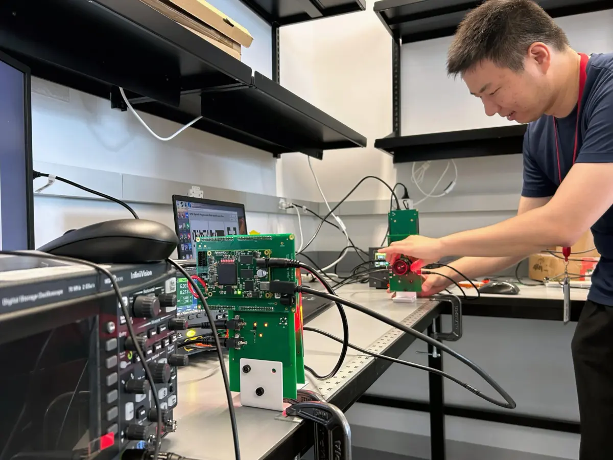
At Cornell Tech’s advanced facilities, the physical manifestation of this breakthrough sits quietly on a lab bench. Postdoctoral researcher Yifan He positions the lens of an optical receiver roughly one meter away from a stationary LED emitting a focused beam of red light. Attached to the receiver, a computer monitor hesitates for a fraction of a second to refresh before displaying a dense array of glowing squares that immediately evoke the visual familiarity of a QR code.
To the casual observer, the setup looks like an advanced optical scanner or a high-speed barcode reader. When a smartphone camera captures a standard QR code, light simply strikes an image sensor as the initial step in a software pipeline designed to decode hidden digital data—typically a simple URL or text string.
The receiver built by He and Seo, however, performs a completely different operational feat. It does not merely read data to open a web browser; it directly alters its own on-chip memory using the precise photocurrents generated by the beamed array of light. Instead of pointing to a website, the optical code directly conveys the complex weights and parameters of an active AI model.
The Honolulu Debut
Following months of rigorous testing, hardware optimization, and calibration tuning, the Cornell Tech team formally introduced their design at the prestigious IEEE/JSAP Symposium on VLSI Technology & Circuits in Honolulu, Hawaii.
The presentation detailed how shining structured data down onto specialized processors could fundamentally sidestep the energy penalties associated with electrical data buses. By targeting data centers, autonomous vehicles, and edge applications—such as AI-powered robots operating in complex environments—the research team positioned their work as a timely intervention for an industry racing toward energy exhaustion.
Supporting Context & Metrics: Decoding the Hardware Architecture
To understand why an optical memory link is such a monumental departure from standard computing paradigms, one must examine the physical anatomy of modern microprocessors and the persistent challenges of data movement.
The SRAM vs. DRAM Conundrum
Microprocessors rely on two primary types of random-access memory to function, each offering distinct trade-offs between speed and capacity:
- Static RAM (SRAM): Embedded directly on the processor die, SRAM is exceptionally fast. However, it requires a significant amount of silicon real estate per bit. Consequently, chips cannot house enough SRAM to store an entire independent AI model.
- Dynamic RAM (DRAM): Located off-chip or linked via complex interconnects, DRAM offers vastly superior storage capacity within a smaller physical footprint, but accessing it requires considerably more time and energy.
In traditional setups, the DRAM stores the massive weight matrices of an AI model, which must be constantly fetched by the processor’s SRAM during inference and training.
"People are designing all sorts of different AI chips," explains Jae-sun Seo. "These processors don’t often have room for all the parameters that make up AI models, so the additional data is stored in dynamic RAM. The electrical connections commonly used to move the data between the DRAM and the processor create cost and efficiency concerns when systems scale up. That’s one of the major bottlenecks."
How the Optical Link Operates
The Cornell Tech architecture reorganizes this relationship entirely. In their proposed system, the DRAM resides with an optical transmitter, while the receiver is integrated directly into the processor’s SRAM cells.
These SRAM cells are specially modified to incorporate microscopic photodiodes. When the transmitter beams structured light down onto the array, photons strike each individual photodiode. This interaction generates a localized photocurrent that instantly "flips" the binary values within the SRAM cells, updating the model parameters almost instantaneously.
Overcoming the Alignment Challenge
In real-world operational environments, maintaining absolute, rigid mechanical alignment between an optical transmitter and a receiver is nearly impossible. Vibrations, thermal expansion, and mechanical shifts can easily misalign the optical path.
To solve this, He and Seo built a sophisticated calibration framework directly into the chip’s circuitry. Before transferring raw model data, the system references a standardized data frame containing precise positional information for each pixel. This reference frame allows the receiver to dynamically adjust and verify alignment.

"Ideally the best way is to have direct, point-to-point space between the transmitter and the receiver," Seo notes, "but even if it’s slightly tilted, we have this calibration circuit."
The Speed and Scale Hurdle
Despite the elegance of the concept, the current hardware setup in Cornell Tech’s lab remains a proof-of-concept prototype. The demonstration unit emits a static 14-by-14-bit matrix by projecting light through a physical metal mask placed over the LED source.
For the technology to be viable in commercial applications, the researchers must scale up to dynamic optical transmitters capable of modulating the light matrix millions of times per second—achieving data transfer rates in the gigabits-per-second range. To achieve this, Seo and He are actively collaborating with specialized optics research groups to develop high-speed spatial light modulators and vertical-cavity surface-emitting laser (VCSEL) arrays.
Official Statements and Expert Analysis
The broader semiconductor and computer engineering community has taken careful note of Cornell Tech’s approach, balancing enthusiasm for its ingenuity with pragmatic skepticism regarding its path to commercialization.
Dennis Sylvester, an IEEE Fellow and chair of the electrical and computer engineering department at the University of Michigan, who was not involved in the research, underscored the scale of the problem the team is trying to solve.
"This is a really important problem," Sylvester states. "It’s got massive commercial implications. This solution is a clever way of dealing with it."
However, Sylvester is quick to point out the formidable physical engineering challenges that still lie ahead. In its current iteration, the technology faces a steep miniaturization barrier: the individual photosensitive bit cells developed by the Cornell team are physically larger than traditional SRAM bit cells found in commercial microprocessors.
Because these photosensitive cells take up more silicon area, a chip equipped with this optical receiver layout would inherently house less total memory—a density trade-off that could potentially neutralize the energy efficiency gains achieved by removing metal wires.
Addressing this critique, Seo emphasizes that cell shrinkage is the primary focus of the group’s ongoing development roadmap. By optimizing transistor geometries, refining circuit layouts, and aggressively leveraging advanced complementary metal-oxide-semiconductor (CMOS) scaling techniques, the team aims to bring the footprint of the optical bit cells down to competitive commercial standards.
Looking ahead at the macroeconomic trends of the tech sector, Sylvester predicts a massive shift in industry focus over the coming years.
"Edge AI is a big growth area, and in three, four, five years, you’re going to hear as much about that as you are with data centers, probably, as the intelligence migrates more and more into these devices that we have," Sylvester remarks.
Future Outlook: Illuminating the Path for Edge AI and Robotics
As artificial intelligence systems transition out of massive, climate-controlled server farms and into dynamic physical environments, the constraints of power consumption and real-time adaptability become paramount. The work being pioneered by Yifan He and Jae-sun Seo points toward a future where hardware architecture can natively ingest updates via light.
Transforming Robotics and Industrial Automation
Consider the operational reality of modern automated warehouses and smart factories. Fleet management systems frequently deploy swarms of autonomous mobile robots (AMRs) that must constantly adapt to changing floor plans, new inventory layouts, and updated operational safety parameters.
Today, updating the AI models governing these robots requires docking stations, high-speed Wi-Fi or tethered cable connections, and substantial energy expenditure as local processors write new weights into memory. With an optical updating link, a robot could simply drive underneath an overhead optical transmitter—much like an electric vehicle plugging into a supercharger—and receive a complete, high-bandwidth AI model update flashed directly into its SRAM memory in milliseconds.
The Promise for Microrobotics
Beyond industrial AMRs, the long-term implications extend even further into the realm of microrobotics. Microscale robots are inherently bottlenecked by their physical dimensions; carrying heavy batteries, complex wiring harnesses, or bulky communication transceivers is physically impossible at millimeter scales.
While adapting optical receiver technology to microrobots will require extreme, size-conscious engineering and further breakthroughs in micro-optics, the prospect of beaming power and cognitive updates directly to untethered microscopic machines represents a tantalizing horizon for the field.
Conclusion
The convergence of optics and electronics has long been viewed as the holy grail of high-performance computing. While obstacles remain in scaling down photosensitive cell sizes and achieving commercial gigabit-per-second modulation speeds, Cornell Tech’s optically programmable receiver demonstrates that moving beyond copper wires is not only possible, but increasingly necessary.
As edge computing continues its explosive growth, the ability to flash intelligence directly onto silicon via beams of light may soon evolve from a clever lab-bench demonstration into the foundational nervous system of autonomous machines.
